MX23L6410ATC-90G
MX23L6410ATC-90G is 64M-BIT PAGE MODE MASK ROM manufactured by Macronix.
- Part of the MX23L6410A comparator family.
- Part of the MX23L6410A comparator family.
Features
- Bit organization
- 8M x 8 (byte mode)
- 4M x 16 (word mode)
- Fast access time
- Random access:70ns (max.)
- Page access:25ns (max.)
- Page size
- 8 words per page
- Current
- Operating:20mA
- Standby:15uA
- Supply voltage
- 2.7V ~ 3.6V
- Package
- 48 pin TSOP (12mm x 20mm)
- Temperature
- 0°C ~ 70°C
- Process
- 0.18um
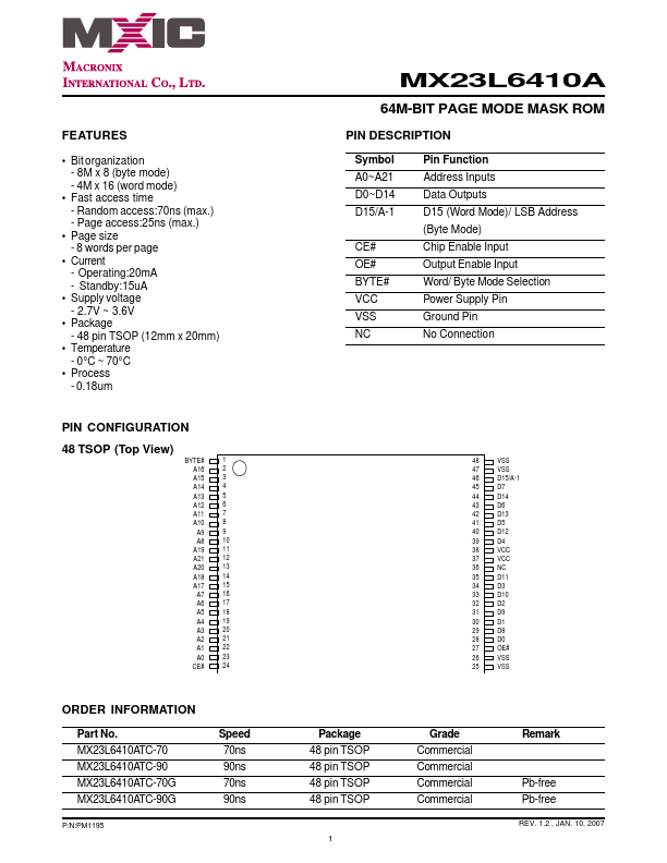
PIN CONFIGURATION
48 TSOP (Top View)
BYTE# A16 A15 A14 A13 A12 A11 A10 A9 A8 A19 A21 A20 A18 A17 A7 A6 A5 A4 A3 A2 A1 A0 CE#
1 2 3 4 5 6 7 8 9 10 11 12 13 14 15 16 17 18 19 20 21 22 23 24
ORDER INFORMATION
Part No. MX23L6410ATC-70 MX23L6410ATC-90 MX23L6410ATC-70G MX23L6410ATC-90G
P/N:PM1195
Speed 70ns 90ns 70ns 90ns
MX23L6410A
64M-BIT PAGE MODE MASK...