MDD3752RH
MDD3752RH is P-Channel Trench MOSFET manufactured by MagnaChip.
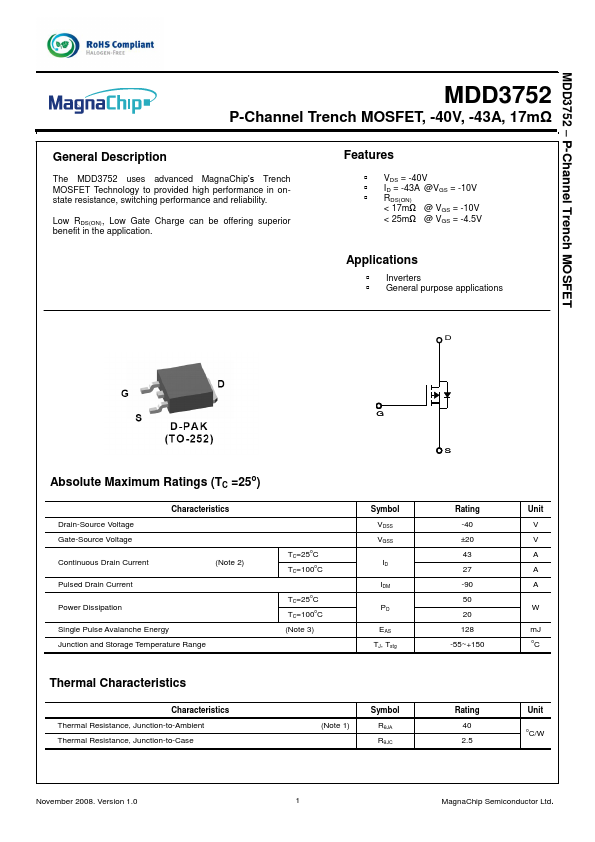
Description
The MDD3752 uses advanced Magna Chip’s Trench MOSFET Technology to provided high performance in onstate resistance, switching performance and reliability. Low RDS(ON), Low Gate Charge can be offering superior benefit in the application.
Features
VDS = -40V ID = -43A @VGS = -10V RDS(ON) < 17mΩ @ VGS = -10V < 25mΩ @ VGS = -4.5V
Applications
Inverters General purpose applications
Absolute Maximum Ratings (TC =25o)
Characteristics Drain-Source Voltage Gate-Source Voltage Continuous Drain Current Pulsed Drain Current Power Dissipation Single Pulse Avalanche Energy Junction and Storage Temperature Range TC=25 C TC=100 C (Note 3) o o
Symbol VDSS VGSS
Rating -40 ±20 43
Unit V V A A A W
(Note 2)
TC=25 C TC=100 C o o
ID IDM PD EAS TJ, Tstg
27 -90 50 20 128 -55~+150 m J o
Thermal Characteristics
Characteristics Thermal Resistance, Junction-to-Ambient Thermal Resistance, Junction-to-Case (Note 1) Symbol RθJA RθJC Rating 40 2.5 Unit o
C/W
November 2008. Version 1.0
Magna Chip Semiconductor Ltd.
MDD3752
- P-Channel Trench MOSFET
Ordering Information
Part Number MDD3752RH Temp. Range -55~150o C Package D-PAK Packing Tape & Reel Ro HS Status Halogen Free
Electrical Characteristics (TJ =25o C unless otherwise noted)
Characteristics Static Characteristics Drain-Source Breakdown Voltage Gate Threshold Voltage Zero Gate Voltage Drain Current Gate Leakage Current Drain-Source ON Resistance Forward Transconductance Dynamic Characteristics Total Gate Charge Gate-Source Charge Gate-Drain Charge Input Capacitance Reverse Transfer Capacitance Output Capacitance Turn-On Delay Time Turn-On Rise Time Turn-Off Delay Time Turn-Off Fall Time Drain-Source Body Diode Characteristics Source-Drain Diode Forward Voltage Reverse Recovery Time Reverse Recovery Charge
Note : 1. 2. 3. Surface mounted RF4 board with 2oz. Copper. PD is based on TJ(MAX)=150OC, PD(TC=25OC) is based on Rθ JC. Starting TJ=25°C, L=1m H, IAS=-16A VDD=-20V, VGS=-10V
Symbol
Test...