ME1303AT3-G Description
The ME1303AT3 is the P-Channel logic enhancement mode power field effect transistors are produced using high cell density , DMOS trench technology. This high density process is especially tailored to minimize on-state resistance. These devices are particularly suited for low voltage application such as cellular phone and notebook puter power management and other battery powered circuits where high-side switching and...
ME1303AT3-G Key Features
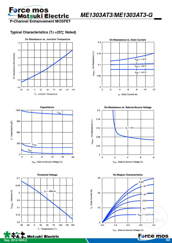
- 20V/-3.4A,RDS(ON)=95mΩ@VGS=-4.5V
- 20V/-2.4A,RDS(ON)=120mΩ@VGS=-2.5V
- 20V/-1.7A,RDS(ON)=180mΩ@VGS=-1.8V
- Super high density cell design for extremely low RDS(ON)
- Exceptional on-resistance and maximum DC current
ME1303AT3-G Applications
- Power Management in Note book