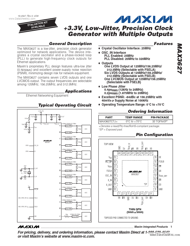
MAX3627
MAX3627 is Precision Clock Generator manufactured by Maxim Integrated.
19-4567; Rev 0; 4/09
..
KIT ATION EVALU E L B AVAILA
+3.3V, Low-Jitter, Precision Clock Generator with Multiple Outputs
General Description Features
- Crystal Oscillator Interface: 25MHz
- OSC_IN Interface PLL Enabled: 25MHz PLL Disabled: 20MHz to 320MHz
- Outputs One LVDS Output at 125MHz/156.25MHz/ 312.5MHz (Selectable with FSELA) Six LVDS Outputs at 125MHz/156.25MHz/ 312.5MHz (Selectable with FSELB) One LVCMOS Output at 125MHz/156.25MHz (Selectable with FSELB)
- Low Phase Jitter 0.4ps RMS (12k Hz to 20MHz) 0.2ps RMS (1.875MHz to 20MHz)
- Excellent PSNR: -64d Bc at 156.25MHz with 40m VP-P Supply Noise at 100k Hz
- Operating Temperature Range: 0°C to +70°C
The MAX3627 is a low-jitter, precision clock generator optimized for network applications. The device integrates a crystal oscillator and a phase-locked loop (PLL) to generate high-frequency clock outputs for Ethernet applications. Maxim’s proprietary PLL design Features ultra-low jitter (0.4ps RMS) and excellent power-supply noise rejection (PSNR), minimizing design risk for network equipment. The MAX3627 contains seven LVDS outputs and one LVCMOS output. The output frequencies are selectable among 125MHz, 156.25MHz, and 312.5MHz.
Applications
Ethernet Networking Equipment
Typical Operating Circuit
+3.3V ±5% 0.1μF 0.1μF 0.1μF
Ordering Information
PART MAX3627CTJ+ TEMP RANGE 0°C to +70°C PIN-PACKAGE 32 TQFN-EP-
VDDO_SE Q0 125MHz/156MHz/312.5MHz Z0 = 50Ω 100Ω Q0 Z0 = 50Ω ASIC
10.5Ω
10μF VDDA 0.01μF
VDDO_DIFF
+Denotes a lead(Pb)-free/Ro HS-pliant package.
- EP = Exposed pad.
125MHz/156MHz/312.5MHz Z0 = 50Ω Q1
Pin Configuration
TOP VIEW
GND Q7 VDDO_SE VDDO_DIFF
100Ω ASIC
MAX3627 OPEN OSC_IN Q1 Z0 = 50Ω 125MHz/156MHz/312.5MHz Z0 =...