MAX3637
MAX3637 is Programmable Clock Generator manufactured by Maxim Integrated.
19-4909; Rev 0; 10/09
..
Low-Jitter, Wide Frequency Range, Programmable Clock Generator with 10 Outputs
General Description
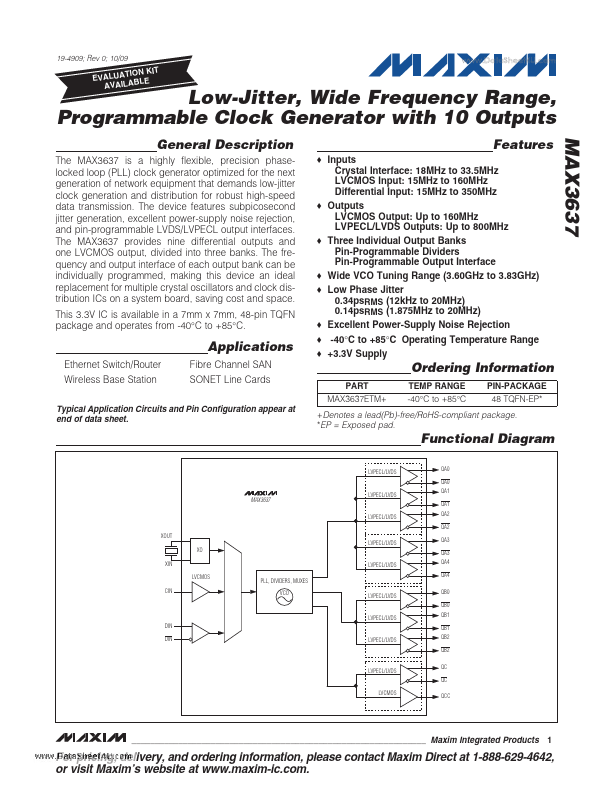
The MAX3637 is a highly flexible, precision phaselocked loop (PLL) clock generator optimized for the next generation of network equipment that demands low-jitter clock generation and distribution for robust high-speed data transmission. The device Features subpicosecond jitter generation, excellent power-supply noise rejection, and pin-programmable LVDS/LVPECL output interfaces. The MAX3637 provides nine differential outputs and one LVCMOS output, divided into three banks. The frequency and output interface of each output bank can be individually programmed, making this device an ideal replacement for multiple crystal oscillators and clock distribution ICs on a system board, saving cost and space. This 3.3V IC is available in a 7mm x 7mm, 48-pin TQFN package and operates from -40°C to +85°C.
TION KIT EVALUA BLE IL AVA A
Features
S Inputs Crystal Interface: 18MHz to 33.5MHz LVCMOS Input: 15MHz to 160MHz Differential Input: 15MHz to 350MHz S Outputs LVCMOS Output: Up to 160MHz LVPECL/LVDS Outputs: Up to 800MHz S Three Individual Output Banks Pin-Programmable Dividers Pin-Programmable Output Interface S Wide VCO Tuning Range (3.60GHz to 3.83GHz) S Low Phase Jitter 0.34ps RMS (12k Hz to 20MHz) 0.14ps RMS (1.875MHz to 20MHz) S Excellent Power-Supply Noise Rejection S -40NC to +85NC Operating Temperature Range S +3.3V Supply
Applications
Ethernet Switch/Router Wireless Base Station Fibre Channel SAN SONET Line Cards
Ordering Information
PART MAX3637ETM+ TEMP RANGE -40NC to +85NC PIN-PACKAGE 48 TQFN-EP-
Typical Application Circuits and Pin Configuration appear at end of data sheet.
+Denotes a lead(Pb)-free/Ro HS-pliant package.
- EP = Exposed pad.
Functional Diagram
LVPECL/LVDS QA0 QA0
LVPECL/LVDS
QA1 QA1
LVPECL/LVDS XOUT XO XIN LVCMOS CIN PLL, DIVIDERS, MUXES VCO LVPECL/LVDS...