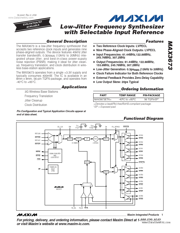
MAX3673
Overview
- Two Reference Clock Inputs: LVPECL
- Nine Phase-Aligned Clock Outputs: LVPECL
- Input Frequencies: 61.44MHz,122.88MHz, 245.76MHz, 307.2MHz
- Output Frequencies: 61.44MHz, 122.88MHz, 153.6MHz, 245.76MHz, 307.2MHz
- Low-Jitter Generation: 0.3psRMS (12kHz to 20MHz)
- Clock Failure Indicator for Both Reference Clocks
- External Feedback Provides Zero-Delay Capability
- Low Output Skew: 20ps Typical MAX3673 The MAX3673 is a low-jitter frequency synthesizer that accepts two reference clock inputs and generates nine phase-aligned outputs. The device features 40kHz jitter transfer bandwidth, 0.3psRMS (12kHz to 20MHz) integrated phase jitter, and best-in-class power-supply noise rejection (PSNR), making it ideal for jitter cleanup, frequency translation, and clock distribution in wireless base-station applications. The MAX3673 operates from a single +3.3V supply and typically consumes 400mW. The IC is available in an 8mm x 8mm, 56-pin TQFN package, and operates from -40°C to +85°C.