• Part: MAX4885
  • Description: Complete VGA 1:2 or 2:1 Multiplexer
  • Manufacturer: Maxim Integrated
  • Size: 404.18 KB
Download MAX4885 Datasheet PDF
Maxim Integrated
MAX4885
MAX4885 is Complete VGA 1:2 or 2:1 Multiplexer manufactured by Maxim Integrated.
19-0554; Rev 0; 5/06 plete VGA 1:2 or 2:1 Multiplexer General Description 
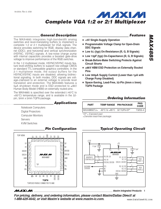
The MAX4885 integrates high-bandwidth analog switches and level-translating buffers to implement a plete 1:2 or 2:1 multiplexer for VGA signals. The device provides switching for RGB, display data channel (DDC), and horizontal and vertical synchronization (HSYNC, VSYNC) signals. A low-noise charge pump with internal capacitors provides a boosted gate-drive voltage to improve performance of the RGB switches. In the 1:2 multiplexer mode, HSYNC/VSYNC inputs feature level-shifting buffers to support low-voltage CMOS or standard TTL-patible graphics controllers. In the 2:1 multiplexer mode, the output buffers for the HSYNC/VSYNC inputs are disabled, allowing bidirectional signaling. In both modes, DDC signals are voltage-clamped to an external voltage to provide level translation and protection. The MAX4885 Features a 5µA shutdown mode and is ESD protected to ±8k V Human Body Model (HBM) on externally routed pins. The MAX4885 is specified over the extended (-40°C to +85°C) temperature range, and is available in the 32pin, 5mm x 5mm TQFN package. .. Features - +5V Single-Supply Operation - Programmable Voltage Clamp for Open-Drain DDC Signals - Low 5Ω (typ) On-Resistance (R, G, B Signals) - Low 13p F (typ) On-Capacitance (R, G, B Signals) - Break-Before-Make Switching Protects Against Circuit Shorts - ±8k V HBM ESD Protection on Externally Routed Pins - Low 300µA Supply Current (Lower than 1µA with Charge Pump Disabled) - Space-Saving, Lead-Free, 32-Pin (5mm x 5mm) TQFN Package Ordering Information PART MAX4885ETJ+ TEMP RANGE PIN-PACKAGE PKG CODE T3255-4 Applications Notebook puters Digital Projectors puter Monitors Servers KVM Switches -40°C to +85°C 32 TQFN-EP- - EP = Exposed pad. +Denotes lead-free package. Pin Configuration H1 H2 V1 B1 V+ V2 B2 Typical Operating Circuit TOP VIEW 24 G1 25 R1 26 DDCB1 27 DDCA1 28 GND 29 V+ 30 M 31 SEL 32 1...