GENERAL DESCRIPTION
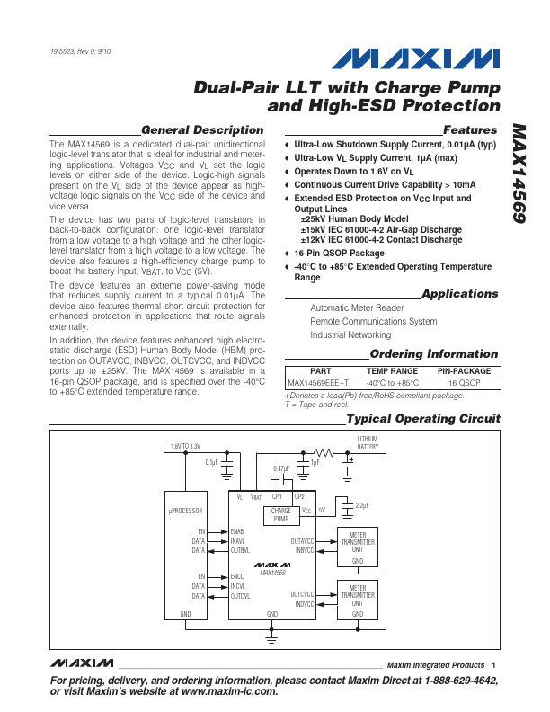
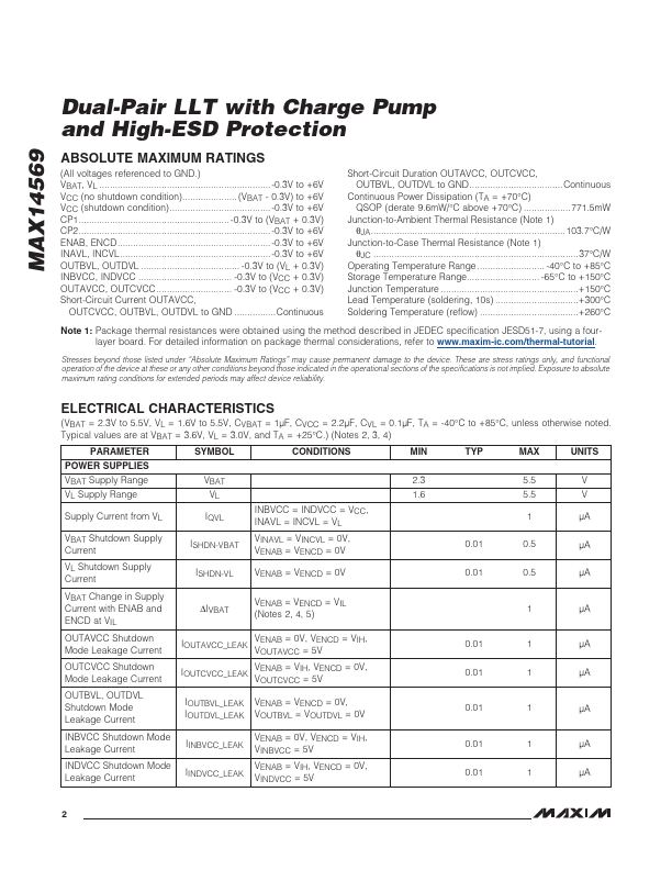
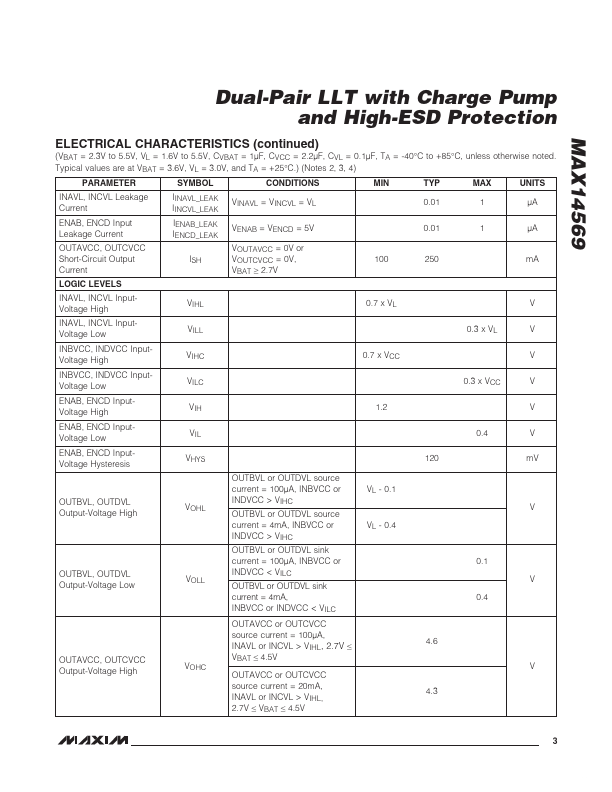
Voltages VCC and VL set the logic levels on either side of the device. Logic-high signals present on the VL side of the device appear as highvoltage logic signals on the VCC side of the device and vice versa. The device features an extreme power-saving mode that reduces supply current to a typical 0.01FA. The device also features thermal short-circuit protection for enhanced protection in applications that route signals externally. In addition, the device features enhanced high electrostatic discharge (ESD) Human Body Model (HBM) protection on OUTAVCC, INBVCC, OUTCVCC, and INDVCC ports up to Q25kV. The MAX14569 is available in a 16-pin QSOP package, and is specified over the -40NC to +85NC extended temperature range. FEATURES
S Ultra-Low Shutdown Supply Current, 0.01µA (typ) S Ultra-Low VL Supply Current, 1µA (max) S Operates Down to 1.6V on VL S Continuous Current Drive Capability > 10mA S Extended ESD Protection on VCC Input and MAX14569 Output Lines ±25kV Human B... Maxim Integrated