GENERAL DESCRIPTION
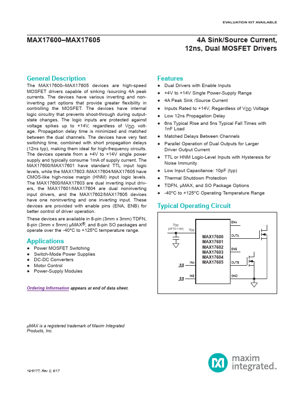
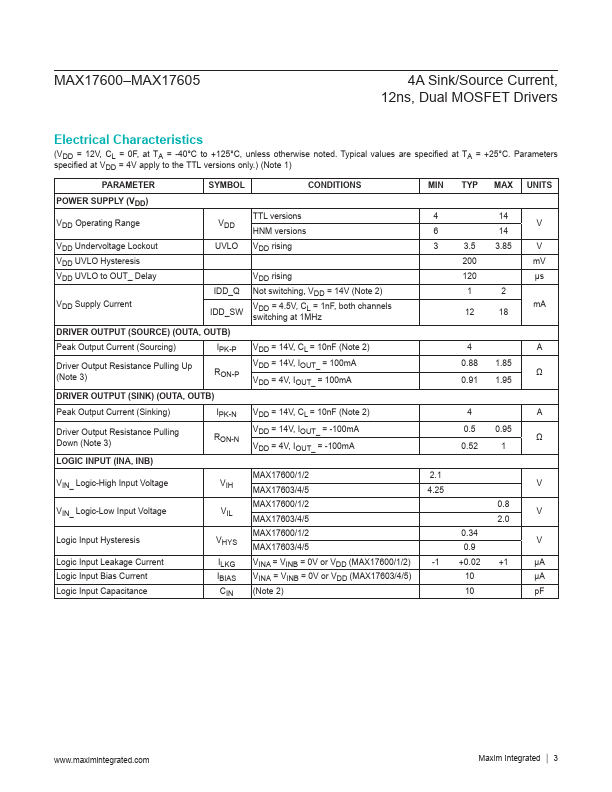
The logic inputs are protected against voltage spikes up to +14V, regardless of VDD voltage. Propagation delay time is minimized and matched between the dual channels. The devices have very fast switching time, combined with short propagation delays (12ns typ), making them ideal for high-frequency circuits. The devices operate from a +4V to +14V single power supply and typically consume 1mA of supply current. The MAX17601/ MAX17602 have standard TTL input logic levels, while the MAX17603 /MAX17604/MAX17605 have CMOS-like highnoise margin (HNM) input logic levels. The MAX17603 is a dual inverting input driver, the MAX17601/MAX17604 are dual noninverting input drivers, and the MAX17602 / MAX17605 devices have one noninverting and one inverting input. These devices are provided with enable pins (ENA, ENB) for better control of driver operation. These devices are available in an 8-pin (3mm x 3mm) TDFN and 8-pin SO packages and operate over the -40NC to +125NC temperature range. Maxim Integrated