MIC5162 Overview
Key Specifications
Package: MSOP
Mount Type: Surface Mount
Pins: 10
Max Operating Temp: 125 °C
Key Features
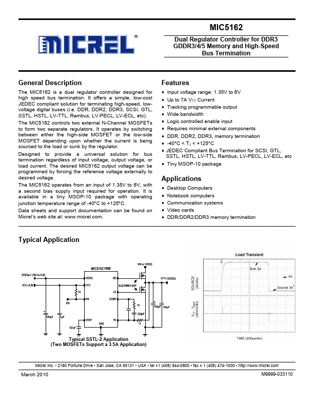
- Input voltage range: 1.35V to 6V high speed bus termination. It offers a simple, low-cost
- Up to 7A VTT Current JEDEC compliant solution for terminating high-speed, low
- Tracking programmable output voltage digital buses (i.e. DDR, DDR2, DDR3, SCSI, GTL
- Wide bandwidth SSTL, HSTL, LV-TTL, Rambus, LV-PECL, LV-ECL, etc)
- Logic controlled enable input The MIC5162 controls two external N-Channel MOSFETs
- DDR, DDR2, DDR3, memory termination MOSFET depending upon whether the current is being
- 40°C < TJ < +125°C sourced to the load or sunk by the regulator
- Desktop Computers a second bias supply input required for operation. It is
- Notebook computers available in a tiny MSOP-10 package with operating
- Communication systems junction temperature range of -40°C to +125°C