SY10H842L
SY10H842L is 3.3V SINGLE SUPPLY QUAD PECL-TO-TTL OUTPUT ENABLE manufactured by Micrel Semiconductor.
..
3.3V SINGLE SUPPLY QUAD PECL-TO-TTL OUTPUT ENABLE
Features s s s s s s s s s s s s 3.3V power supply Translates positive ECL-to-TTL (PECL-to-TTL) 300ps pin-to-pin skew 500ps part-to-part skew Differential internal design for increased noise immunity and stable threshold inputs VBB reference output Single supply Enable input Extra TTL and ECL power/ground pins to reduce cross-talk/noise High drive capability: 24m A each output Fully patible with industry standard 10K, 100K I/O levels Available in 16-pin SOIC package
Clock Works™ PRELIMINARY SY10H842L SY100H842L
DESCRIPTION
The SY10/100H842L are single supply, low skew translating 1:4 clock drivers. The devices feature a 24m A TTL output stage, with AC performance specified into a 20p F load capacitance. A HIGH on the enable pin (EN) forces all outputs LOW. As frequencies increase to 40MHz and above, precise timing and shaping of clock signals bees extremely important. The H842 solves several clock distribution problems such as minimizing skew 300ps), maximizing clock fanout (24m A drive), and precise duty cycle control through a proprietary differential internal design. The 10K version is patible with 10KH ECL logic levels. The 100K version is patible with 100K levels.
BLOCK DIAGRAM
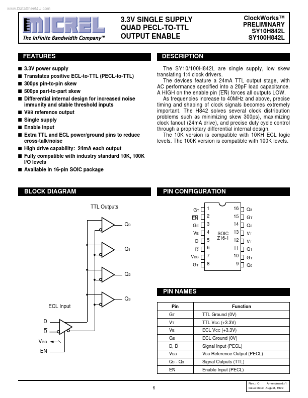
TTL Outputs
PIN CONFIGURATION
GT EN 1 2 3 4 5 6 7 8 SOIC Z16-1 16 15 14 13 12 11 10 9 Q3 GT Q2 VT VT Q1 GT Q0
Q0
GE VE D
Q1
D VBB GT
Q2
PIN NAMES
Q3 ECL Input D D VBB EN
Pin GT VT VE GE D, D VBB Q0
- Q3 EN Function TTL Ground (0V) TTL VCC (+3.3V) ECL VCC (+3.3V) ECL Ground (0V) Signal Input (PECL) VBB Reference Output (PECL) Signal Outputs (TTL) Enable Input (PECL)
Rev.: C Amendment: /1
Issue Date: August, 1999
Micrel
Clock Works™ PRELIMINARY SY10H842L SY100H842L
TRUTH TABLE
D L H X EN L L H Q L H L
PIN DESCRIPTION
Pin 1 2 3 4 Symbol GT EN GE VE D D VBB GT Q0 GT Q1 VT VT Q2 GT Q3 Description TTL Ground (0V) Enable Input (PECL) ECL Ground (0V) ECL VCC (+3.3V) ECL Signal Input (Non-inverting)...