SY89847U
SY89847U is LVDS 1:5 Fanout manufactured by Micrel Semiconductor.
1.5GHz Precision, LVDS 1:5 Fanout with 2:1 MUX and Fail Safe Input with Internal Termination
General Description
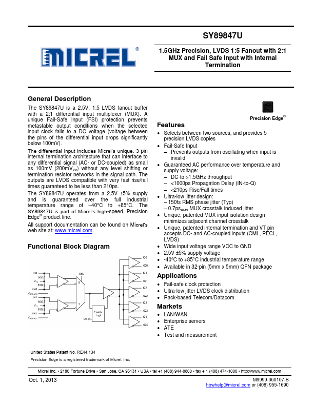
The SY89847U is a 2.5V, 1:5 LVDS fanout buffer with a 2:1 differential input multiplexer (MUX). A unique Fail-Safe Input (FSI) protection prevents metastable output conditions when the selected input clock fails to a DC voltage (voltage between the pins of the differential input drops significantly below 100m V). The differential input includes Micrel’s unique, 3-pin internal termination architecture that can interface to any differential signal (AC- or DC-coupled) as small as 100m V (200m VPP) without any level shifting or termination resistor networks in the signal path. The outputs are LVDS patible with very fast rise/fall times guaranteed to be less than 210ps.
The SY89847U operates from a 2.5V ±5% supply and is guaranteed over the full industrial temperature range of
- 40°C to +85°C. The SY89847U is part of Micrel’s high-speed, Precision Edge® product line. All support documentation can be found on Micrel’s web site at: .micrel..
Functional Block Diagram
Features
Precision Edge®
- Selects between two sources, and provides 5 precision LVDS copies
- Fail-Safe Input
- Prevents outputs from oscillating when input is invalid
- Guaranteed AC performance over temperature and supply voltage:
- DC-to >1.5GHz throughput
- <1000ps Propagation Delay (IN-to-Q)
- <210ps Rise/Fall times
- Ultra-low jitter design:
- 150fs RMS phase jitter (Typ)
- 0.7ps RMS MUX crosstalk induced jitter
- Unique, patented MUX input isolation design minimizes adjacent channel crosstalk
- Unique, patented internal termination and VT pin accepts DC- and AC-coupled inputs (CML, PECL, LVDS)
- Wide input voltage range VCC to GND
- 2.5V ±5% supply voltage
- -40°C to +85°C industrial temperature range
- Available in 32-pin (5mm x 5mm) QFN package
Applications
- Fail-safe clock protection
- Ultra-low jitter LVDS clock distribution
- Rack-based Tele/Data
Markets
-...