PL133-27 Overview
Key Specifications
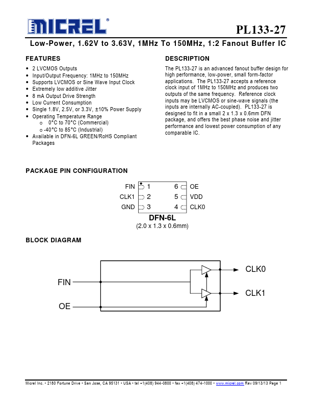
Package: DFN
Mount Type: Surface Mount
Pins: 6
Max Frequency: 150 MHz
Description
The PL133-27 is an advanced fanout buffer design for high performance, low-power, small form-factor applications. The PL133-27 accepts a reference clock input of 1MHz to 150MHz and produces two outputs of the same frequency.
Key Features
- 2 LVCMOS Outputs
- Input/Output Frequency: 1MHz to 150MHz
- Supports LVCMOS or Sine Wave Input Clock
- Extremely low additive Jitter
- 8 mA Output Drive Strength
- Low Current Consumption
- Single 1.8V, 2.5V, or 3.3V, ±10% Power Supply
- Operating Temperature Range o 0°C to 70°C (Commercial) o -40°C to 85°C (Industrial)
- Available in DFN-6L GREEN/RoHS Compliant Packages