FEATURES
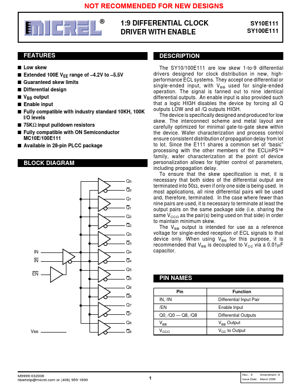
s Low skew s Extended 100E VEE range of –4.2V to –5.5V s Guaranteed skew limits s Differential design s VBB output s Enable input s Fully compatible with industry standard 10KH, 100K I/O levels s 75KΩ input pulldown resistors s Fully compatible with ON Semiconductor MC10E/100E111 s Available in 28-pin PLCC package BLOCK DIAGRAM Q0 Q0 Q1 Q1 Q2 Q2 Q3 Q3 IN Q4 IN Q4 Q5 EN Q5 Q6 Q6 Q7 Q7 Q8 VBB Q8 DESCRIPTION
An enable input is also provided such that a logic HIGH disables the device by forcing all Q outputs LOW and all /Q outputs HIGH. The device is specifically designed and produced for low skew. The interconnect scheme and metal layout are carefully optimized for minimal gate-to-gate skew within the device. Wafer characterization and process control ensure consistent distribution of propagation delay from lot to lot. Since the E111 shares a common set of “basic” processing with the other members of the ECLinPS™ family, wafer characterization at the point of device personalization allows for tighter control of parameters, including propagation delay. Micrel