FEATURES
s 600ps max. propagation delay s Extended 100E VEE range of –4.2V to –5.5V s Common enable input s Fully compatible with industry standard 10KH, 100K I/O levels s Internal 75KΩ input pulldown resistors s Fully compatible with Motorola MC10E/100E112 s Available in 28-pin PLCC package DESCRIPTION
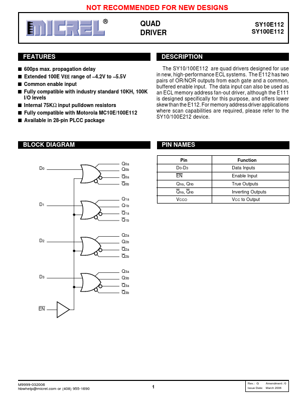
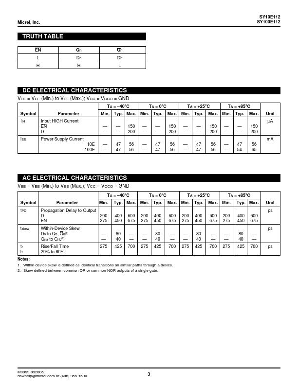
For memory address driver applications where scan capabilities are required, please refer to the SY10/100E212 device. BLOCK DIAGRAM D0 D1 D2 D3 EN PIN NAMES Pin Q0a Q0b D0-D3 Q0a EN Q0b Qna, Qnb Qna, Qnb Q1a VCCO Q1b Q1a Q1b Q2a Q2b Q2a Q2b Q3a Q3b Q3a Q3b Function Data Inputs Enable Input True Outputs Inverting Outputs VCC to Output M9999-032006 hbwhelp@micrel.com or (408) 955-1690 1 Rev.: G Amendment: /0 Issue Date: March 2006 Micrel, Inc. SY10E112 SY100E112 PACKAGE/ORDERING INFORMATION Q3b Q3a Q3b Q3a VCCO Q2b Q2a VCCO D3 D2 VEE D1 D0 EN 25 24 23 22 21 20 19 26 18 27 17 28 PLCC 16 1 TOP VIEW 15 2 J28-1 14 3 13 4 12 5 6 7 8 9 10 11 Q2b Q2a VCC Q1b Q1a Q1b Q1a NC VCCO Q0a Q0b Q0a Q0b V... Micrel