FEATURES
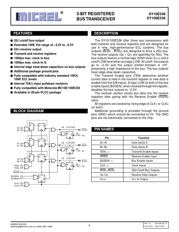
s 25Ω cutoff bus output s Extended 100E VEE range of –4.2V to –5.5V s 50Ω receiver output s Transmit and receive registers s 1500ps max. clock to bus s 1000ps max. clock to Q s Internal edge slow-down capacitors on bus outputs s Additional package ground pins s Fully compatible with industry standard 10KH, 100K ECL levels s Internal 75KΩ input pulldown resistors s Fully compatible with Motorola MC10E/100E336 s Available in 28-pin PLCC package BLOCK DIAGRAM DESCRIPTION
The bus outputs feature a normal logic HIGH level (VOH) and a cutoff LOW level when at a logic LOW. At cutoff, the outputs go to –2.0V and the output emitter-follower is “off”, presenting a high impedance to the bus. The bus outputs have edge slow-down capacitors. The Transmit Enable pins (TEN) determine whether current data is held in the transmit register or new data is loaded from the A/B inputs. A logic LOW on both of the bus enable inputs (BUSEN), when clocked through the register, disables the bus outputs to –2.0V. Micrel