FEATURES
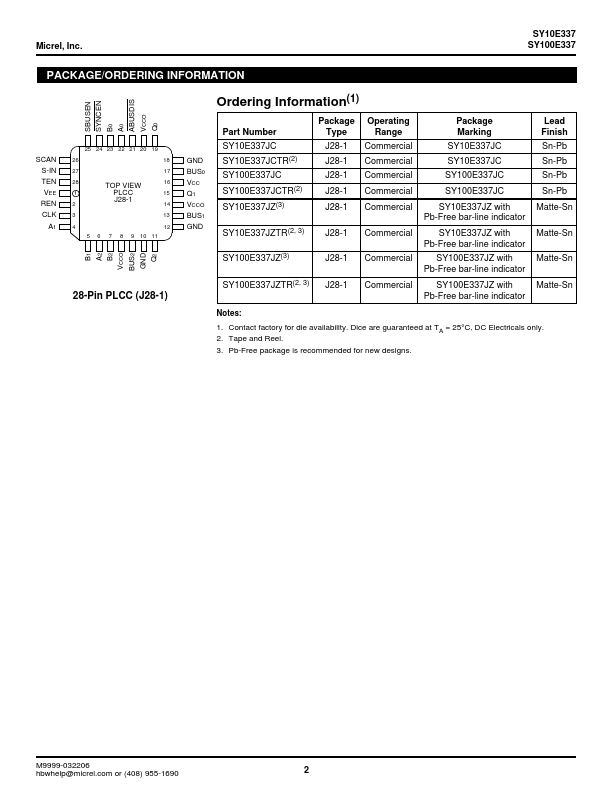
s 1500ps max. clock to bus (data transmit) s 1000ps max. clock to Q (data receive) s Extended 100E VEE range of –4.2V to –5.5V s 25Ω cutoff bus outputs s 50Ω receiver outputs s Scannable implementation of E336 s Synchronous and asynchronous bus enables s Non-inverting data path s Bus outputs feature internal edge slow-down capacitors s Additional package ground pins s Fully compatible with industry standard 10KH, 100K ECL levels s Internal 75KΩ input pulldown resistors s Fully compatible with Motorola MC10E/100E337 s Available in 28-pin PLCC package PIN NAMES Pin A0–A2 B0–B2 S-IN TEN, REN SCAN ABUSDIS SBUSEN SYNCEN CLK BUS0–BUS2 Q0–Q2 VCCO Function Data Inputs A Data Inputs B Serial (Scan) Data Input LOAD/HOLD Controls Scan Control Asynchronous Bus Disable Synchronous Bus Enable Synchronous Enable Control Clock 25Ω Cutoff BUS Outputs Receive Data Outputs (Q2 serves as SCAN_OUT in scan mode) VCC to Output DESCRIPTION
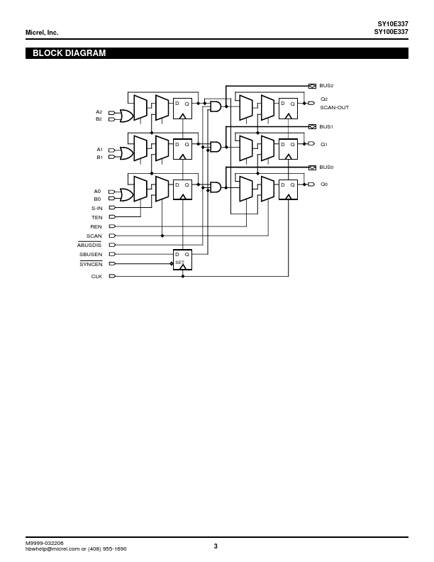
The bus outputs also feature edge slow-down capacitors. Both drive and receive sides feature the same logic, including a loopback path to hold data. Micrel