MT47H64M16
MT47H64M16 is DDR2 SDRAM manufactured by Micron Technology.
- Part of the MT47H256M4 comparator family.
- Part of the MT47H256M4 comparator family.
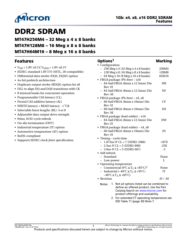
Features
Features
- VDD = 1.8V ±0.1V, VDDQ = 1.8V ±0.1V
- JEDEC-standard 1.8V I/O (SSTL_18-patible)
- Differential data strobe (DQS, DQS#) option
- 4n-bit prefetch architecture
- Duplicate output strobe (RDQS) option for x8
- DLL to align DQ and DQS transitions with CK
- 8 internal banks for concurrent operation
- Programmable CAS latency (CL)
- Posted CAS additive latency (AL)
- WRITE latency = READ latency
- 1 t CK
- Selectable burst lengths (BL): 4 or 8
- Adjustable data-output drive strength
- 64ms, 8192-cycle refresh
- On-die termination (ODT)
- Industrial temperature (IT) option
- Automotive temperature (AT) option
- Ro HS-pliant
- Supports JEDEC clock jitter specification
Options1
- Configuration
- 256 Meg x 4 (32 Meg x 4 x 8 banks)
- 128 Meg x 8 (16 Meg x 8 x 8 banks)
- 64 Meg x...


