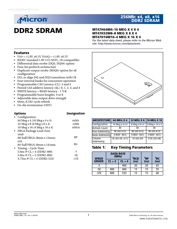
MT47H64M4
MT47H64M4 is DDR2 SDRAM manufactured by Micron Technology.
Features
- -
- -
- -
- -
- -
- -
- - VDD = +1.8V ±0.1V, VDDQ = +1.8V ±0.1V JEDEC standard 1.8V I/O (SSTL_18-patible) Differential data strobe (DQS, DQS#) option Four-bit prefetch architecture Duplicate output strobe (RDQS) option for x8 configuration DLL to align DQ and DQS transitions with CK Four internal banks for concurrent operation Programmable CAS Latency (CL): 3 and 4 Posted CAS additive latency (AL): 0, 1, 2, 3, and 4 WRITE latency = READ latency
- 1 t CK Programmable burst lengths: 4 or 8 Adjustable data-output drive strength 64ms, 8,192-cycle refresh On-die termination (ODT) Designation
64M4 32M8 16M16
MT47H64M4- 16 MEG X 4 X 4 MT47H32M8- 8 MEG X 8 X 4 MT47H16M16- 4 MEG X 16 X 4
For the latest data sheet, please refer to the Micron Web site: http://.micron./datasheets
Options
- Configuration 64 Meg x 4 (16 Meg x 4 x 4) 32 Meg x 8 (8 Meg x 8 x 4) 16 Meg x 16 (4 Meg x 16 x 4)
- FBGA Package Lead-Free x4x8 60-ball FBGA (8mm x 12mm) x16 84-ball FBGA (8mm x 14)mm
- Timing
- Cycle Time 5.0ns @ CL = 4 (DDR2-400) 5.0ns @ CL = 3 (DDR2-400) 3.75ns @ CL = 4 (DDR2-533)
ARCHITECTURE
Configuration Refresh Count Row Addressing Bank Addressing
64 MEG X 4
16 Meg x 4 x 4 8K 8K (A0-A12) 4 (BA0
- BA1) 2K (A0-A9, A11)
32 MEG X 8 16 MEG X 16
8 Meg x 8 x 4 8K 8K (A0-A12) 4 (BA0
- BA1) 1K (A0-A9) 4 Meg x 16 x 4 8K 8K (A0-A12) 4 (BA0
- BA1) 512K (A0-A8)
BP BG
Column Addressing
Table 1:
-5 -5E -37E SPEED GRADE -5 -5E -37E
Key Timing Parameters
DATA RATE (MHz) CL = 3
- 400 400 CL = 4 400 400 533 t
RCD (ns) 20 15 15 t RP (ns) t RC (ns)
20 15 15
65 55 60
09005aef80b12a05 256Mb_DDR2_1.fm
- Rev. C 5/04 EN
©2003 Micron Technology, Inc. All rights...