Datasheet4U Logo Datasheet4U.com

MT29F8G08ABCBB - NAND Flash Memory

Download the MT29F8G08ABCBB datasheet PDF. This datasheet also covers the MT29F8G08ABABA variant, as both devices belong to the same nand flash memory family and are provided as variant models within a single manufacturer datasheet.

General Description

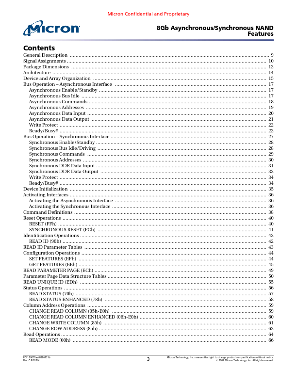
9 Signal Assignments 10 Package Dimensions 12 Architecture 14 Device and Array Organization 15 Bus Operation Asynchronous Interface 17 Asynchronous Enable/Standby 17 Asynchronous Bus Idle 17 Asynchronous Commands 18 Asynchronous Addresses 19 Asynchronous Data Input 20 Asynchrono

Key Features

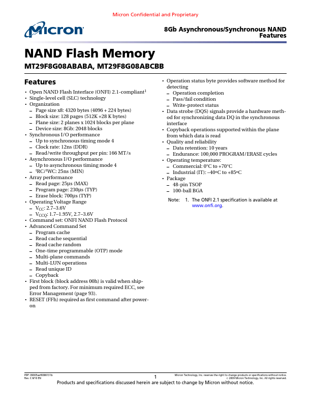
  • NAND Flash Memory MT29F8G08ABABA, MT29F8G08ABCBB Features.
  • Open NAND Flash Interface (ONFI) 2.1-compliant1.
  • Single-level cell (SLC) technology.
  • Organization.
  • Page size x8: 4320 bytes (4096 + 224 bytes).
  • Block size: 128 pages (512K +28 K bytes).
  • Plane size: 2 planes x 1024 blocks per plane.
  • Device size: 8Gb: 2048 blocks.
  • Synchronous I/O performance.
  • Up to synchronous timing mode 4.
  • Clock rate: 12ns (DDR).

📥 Download Datasheet

Note: The manufacturer provides a single datasheet file (MT29F8G08ABABA_Micron.pdf) that lists specifications for multiple related part numbers.

Full PDF Text Transcription (Reference)

The following content is an automatically extracted verbatim text from the original manufacturer datasheet and is provided for reference purposes only.

View original datasheet text
Micron Confidential and Proprietary 8Gb Asynchronous/Synchronous NAND Features NAND Flash Memory MT29F8G08ABABA, MT29F8G08ABCBB Features • Open NAND Flash Interface (ONFI) 2.1-compliant1 • Single-level cell (SLC) technology • Organization – Page size x8: 4320 bytes (4096 + 224 bytes) – Block size: 128 pages (512K +28 K bytes) – Plane size: 2 planes x 1024 blocks per plane – Device size: 8Gb: 2048 blocks • Synchronous I/O performance – Up to synchronous timing mode 4 – Clock rate: 12ns (DDR) – Read/write throughput per pin: 166 MT/s • Asynchronous I/O performance – Up to asynchronous timing mode 4 – tRC/tWC: 25ns (MIN) • Array performance – Read page: 25µs (MAX) – Program page: 230µs (TYP) – Erase block: 700µs (TYP) • Operating Voltage Range – VCC: 2.7–3.6V – VCCQ: 1.7–1.95V, 2.7–3.