APT94N65B2C3G
APT94N65B2C3G is Super Junction MOSFET manufactured by Microsemi.
- Part of the APT94N65B2C3 comparator family.
- Part of the APT94N65B2C3 comparator family.
650V 94A APT94N65B2C3 APT94N65B2C3G-
- G Denotes Ro HS pliant, Pb Free Terminal Finish.
C O OLMOS
Power Semiconductors
Super Junction MOSFET
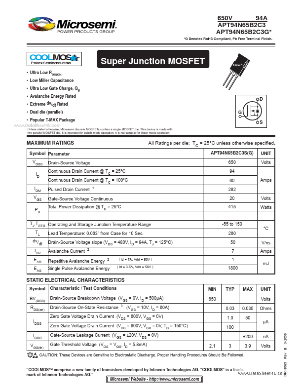
T-Max TM
- Ultra Low RDS(ON)
- Low Miller Capacitance
- Ultra Low Gate Charge, Qg
- Avalanche Energy Rated
- Extreme dv/dt Rated
- Dual die (parallel)
- Popular T-MAX Package ..
Unless stated otherwise, Microsemi discrete MOSFETs contain a single MOSFET die. This device is made with two parallel MOSFET die. It is intended for switch-mode operation. It is not suitable for linear mode operation.
MAXIMUM RATINGS
Symbol Parameter VDSS ID IDM VGS PD Drain-Source Voltage Continuous Drain Current @ TC = 25°C Continuous Drain Current @ TC = 100°C Pulsed Drain Current
All Ratings per die: TC = 25°C unless otherwise specified.
APT94N65B2C3S(G) 650 94 60 282 20 415 Volts Watts Amps UNIT Volts
Gate-Source Voltage Continuous Total Power Dissipation @ TC = 25°C
TJ,TSTG Operating and Storage Junction Temperature Range TL dv/ dt IAR EAR EAS Lead Temperature: 0.063" from Case for 10 Sec. Drain-Source Voltage slope (VDS = 480V, ID = 94A, TJ = 125°C) Avalanche Current
2 2 ( Id = 7A, Vdd = 50V ) ( Id = 3.5A, Vdd = 50V )
-55 to 150 260 50 7 1 1800
°C V/ns Amps m J
Repetitive Avalanche Energy
Single Pulse Avalanche Energy
STATIC ELECTRICAL CHARACTERISTICS
Symbol BV(DSS) RDS(on) IDSS IGSS VGS(th) Characteristic / Test Conditions Drain-Source Breakdown Voltage (VGS = 0V, ID = 500μA) Drain-Source On-State Resistance
MIN 650
UNIT Volts
(VGS = 10V, ID = 60A)
0.03 1.0 100
0.035 50
Ohms μA n A Volts
3-2009 050-8069 Rev B
Zero Gate Voltage Drain Current (VDS = 600V, VGS = 0V) Zero Gate Voltage Drain Current (VDS = 600V, VGS = 0V, TC = 150°C) Gate-Source Leakage Current (VGS = ±20V, VDS = 0V) Gate Threshold Voltage (VDS = VGS, ID = 5.8m A)...