LS3550SA
LS3550SA is General Purpose manufactured by Micross.
Features
:
- Low Output Capacitance Features
3 LEAD TO‐92 PACKAGE ABSOLUTE MAXIMUM RATINGS 1 @ 25°C (unless otherwise noted) Maximum Temperatures Storage Temperature Operating Junction Temperature Maximum Power Dissipation Continuous Power Dissipation Maximum Currents Collector Current Maximum Voltages Collector to Collector Voltage TYP. ‐‐ ‐‐ ‐‐ ‐‐ ‐‐ ‐‐ ‐‐ ‐‐ ‐‐ ‐‐ ‐‐ ‐‐ ‐‐ MAX. ‐‐ ‐‐ ‐‐ ‐‐ ‐‐ ‐‐ ‐‐ ‐0.25 ‐0.2 ‐0.2 2 600 3 UNITS V V V V V n A n A p F MHz d B ‐65°C to +150°C ‐55°C to +150°C TBD 10m A 80V CONDITIONS IC = 10µA, IE = 0 IC = 10µA, IB = 0 IE = 10µA, IC = 02 IC = 10µA, IE = 0 IC = ‐1m A, VCE = ‐5V IC = ‐10m A, VCE = ‐5V IC = ‐100m A, VCE = ‐5V IC = ‐100m A, IB = ‐10m A IE = 0, VCB = ‐3V IE = 0, VCB = ‐30V IE = 0, VCB = ‐10V IC = ‐1m A, VCE = ‐5V
..
ELECTRICAL CHARACTERISTICS @ 25°C (unless otherwise noted) SYMBOL CHARACTERISTICS MIN. BVCBO Collector to Base Voltage ‐45 BVCEO Collector to Emitter Voltage ‐45 BVEBO Emitter‐Base Breakdown Voltage ‐6.2 BVCCO Collector to Collector Voltage ‐80 150 h FE DC Current Gain 120 100 VCE(SAT) Collector Saturation Voltage ‐‐ IEBO Emitter Cutoff Current ‐‐ ICBO Collector Cutoff Current ‐‐ COBO Output Capacitance ‐‐ f T Current Gain Bandwidth ‐‐ Product(Current) NF Narrow Band Noise Figure ‐‐
Click To Buy
IC = ‐100µA, VCE = ‐5V, BW=200Hz, RG= 10Ω, f = 1KHz
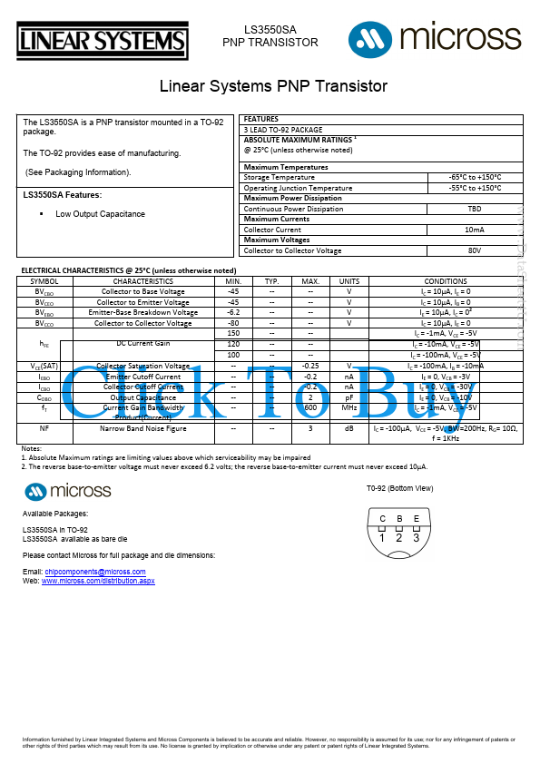
Notes: 1. Absolute Maximum ratings are limiting values above which serviceability may be impaired 2. The reverse base‐to‐emitter voltage must never exceed 6.2 volts; the reverse base‐to‐emitter current must never exceed 10µA. T0-92 (Bottom View)
Available Packages: LS3550SA in TO-92 LS3550SA available as bare die Please contact Micross for full package and die dimensions: Email: chipponents@micross. Web: .micross./distribution.aspx
Information furnished by Linear Integrated Systems and Micross ponents is believed to be accurate and...