FEATURES
G Very High Operating Speed G Operation down to DC with Square Wave Input G Silicon Technology for Low Phase Noise ABSOLUTE MAXIMUM RATINGS
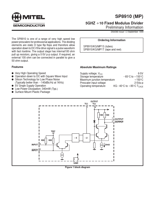
Supply voltage, VCC 6●5V Storage temperature 265°C to 1150°C Maximum junction temperature 1150°C Prescaler input voltage 2●5Vp-p Operating temperature KG240°C to 185°C TCASE (Typically better than 2140dBc/Hz at 1KHz) G 5V Single Supply Operation G Low Power Dissipation: 340mW (Typ.) G Surface Mount Plastic Package VCC 1 OUTPUT VCC 8 100 100 7 6 OUTPUT OUTPUT VREF 45 400 INPUT INPUT 2 3 42 5mA 400 4 4 GND Figure 1 block diagram SP8910 VCC INPUT INPUT GND 1 2 8 7 OUTPUT VCC OUTPUT OUTPUT GND SP8910 3 4 6 5 MP8 Figure 2 Pin connections - top view ELECTRICAL CHARACTERISTICS
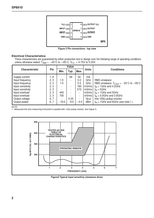
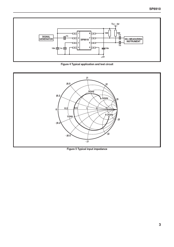
These characteristics are guaranteed by either production test or design over the following range of operating conditions unless otherwise stated: TAMB = 240°C to 185°C, VCC = 4●75V to 5●25V Value Characteristic Supply current Input frequency Input frequency Input sensitivity Input sensitivity Input overload Input overload Output voltage Output power Pin 1, 8 2, 3 2, 3 2, 3 2, 3 2, 3 2, 3 6, 7 6, 7 Min. Mitel Networks