M2V64S40TP
M2V64S40TP is 64M bit Synchronous DRAM manufactured by Mitsubishi Electric.
DESCRIPTION
M2V64S20BTP is organized as 4-bank x4,194,304-word x 4-bit,and M2V64S30BTP is organized as 4-bank x 2097152-word x 8-bit ,and M2V64S40BTP is organized as 4-bank x 1048576-word x 16-bit Synchronous DRAM with LVTTL interface. All inputs and outputs are referenced to the rising edge of CLK. M2V64S20BTP,M2V64S30BTP,M2V64S40BTP achieves very high speed data rates up to 133MHz, and is suitable for main memory or graphic memory in puter systems.
Features
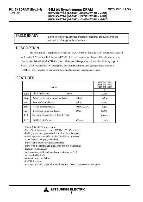
ITEM t CLK t RAS t RCD t AC t RC Icc1 Icc6 Clock Cycle Time (Min.) (Min.) (Min.) (Max.) (CL=3) (Min.) M2V64S20TP M2V64S30TP M2V64S40TP -6 7.5ns 45ns 20.0ns 5.4ns 67.5ns 120m A (Max.) 1m A
Active to Precharge mand Period Row to Column Delay Access Time from CLK Ref/Active mand Period Operation Current (Max.) [Single Bank] Self Refresh Current
- Single 3.3V ±0.3V power supply
- Max. Clock frequency -6 : 133MHz [PC133<3-3-3> ]
- Fully synchronous operation referenced to clock rising edge
- 4-bank operation controlled by BA0,BA1(Bank Address)
- /CAS latency- 2/3 (programmable)
- Burst length- 1/2/4/8/FP (programmable)
- Burst type- Sequential and interleave burst (programmable)
- Random column access
- Auto precharge / All bank precharge controlled by A10
- Auto and self refresh
- 4096 refresh cycles /64ms
- LVTTL Interface
- Package 400-mil, 54-pin Thin Small Outline (TSOP II) with 0.8mm lead pitch
MITSUBISHI ELECTRIC
PC133 SDRAM (Rev.0.5) Oct. '99
64M bit Synchronous DRAM
M2V64S20BTP-6 (4-BANK x 4194304-WORD x 4-BIT) M2V64S30BTP-6 (4-BANK x 2097152-WORD x 8-BIT) M2V64S40BTP-6 (4-BANK x 1048576-WORD x 16-BIT)
MITSUBISHI LSIs
PIN CONFIGURATION (TOP VIEW) M2V64S20BTP M2V64S30BTP M2V64S40BTP
Vdd NC Vdd Q NC DQ0 Vss Q NC NC Vdd Q NC DQ1 Vss Q NC Vdd NC /WE /CAS /RAS /CS BA0(A13) BA1(A12) A10 A0 A1 A2 A3 Vdd Vdd DQ0 Vdd Q NC DQ1 Vss Q NC DQ2 Vdd Q NC DQ3 Vss Q NC Vdd NC /WE /CAS /RAS /CS BA0(A13) BA1(A12) A10 A0 A1 A2 A3 Vdd Vdd DQ0 Vdd Q DQ1 DQ2 Vss Q DQ3 DQ4 Vdd Q DQ5 DQ6 Vss Q DQ7 Vdd DQML /WE /CAS /RAS /CS BA0(A13)...