M5M29GT160BVP
DESCRIPTION
The MITSUBISHI Mobile FLASH M5M29GB/T160BVP are 3.3V-only high speed 16,777,216-bit CMOS boot block Flash Memories with alternating BGO (Back Ground Operation) feature
. The BGO feature of the device allows Program or Erase operations to be performed in one bank while the device simultaneously allows Read operations to be performed on the other bank. This BGO feature is suitable for mobile and personal puting, and munication products. The M5M29GB/T160BVP are fabricated by CMOS technology for the peripheral circuits and DINOR(Divided bit line NOR) architecture for the memory cells, and are available in in 48pin TSOP(I) .
FEATURES
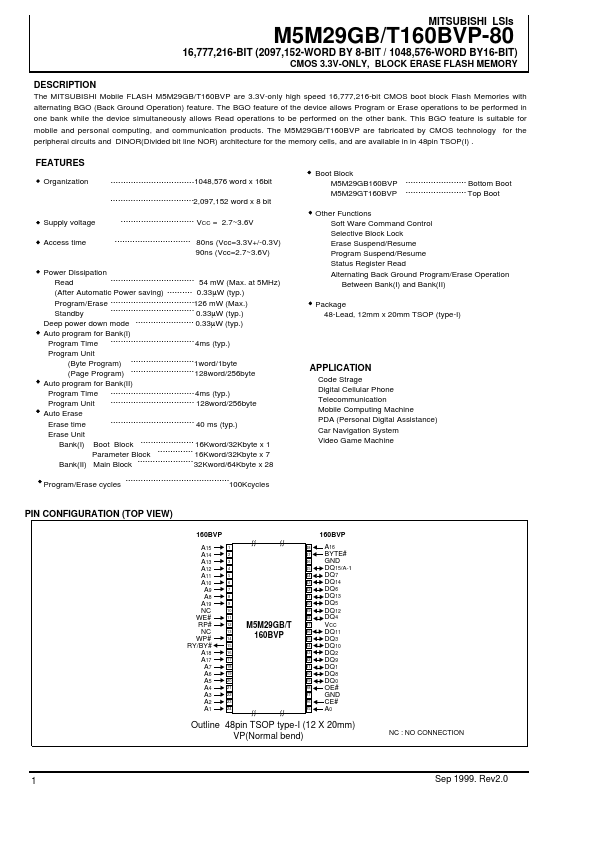
Organization
1048,576 word x 16bit 2,097,152 word x 8 bit
Boot Block M5M29GB160BVP Bottom Boot M5M29GT160BVP Top Boot Other Functions Soft Ware mand Control Selective Block Lock Erase Suspend/Resume Program Suspend/Resume Status...