M65664FP
M65664FP is PICTURE-IN-PICTURE SIGNAL PROCESSING manufactured by Mitsubishi Electric.
MITSUBISHI DIGITAL TV ICs
PICTURE-IN-PICTURE SIGNAL PROCESSING DESCRIPTION
The M65664FP is a PIP (Picture in Picture) signal processing LSI, whose sub-picture input is posite signal for NTSC, PAL-M, and PAL-N. The built-in field memory (168k-bit RAM) , V-chip data slicer and analog circuitries lead the high quality PIP system low cost and small size.
APPLICATION
NTSC, PAL-M, PAL-N color TV
REMENDED OPERATING CONDITIONS
Supply voltage range ------------------------ 3.2 ~ 3.5 V Operating frequency ----------------------- 14.32 MHz Operating temperature ------------------------ 0 ~ 70 deg. Input voltage (CMOS interface) "H" ----- VDD x 0.7 ~ VDD V "L" ----- 0 ~ VDD x 0.3 V Output current ( output buffer ) ------------ 4 m A ( MAX ) Output load capacitance ---------------------- 20 p F ( MAX )
- 1 Circuit current ----------------------------------- m A
Features
- Internal V-chip data slicer (for sub-picture) NOTICE: Connect a 0.1µF or larger capacitor between VDD and VSS pins.
- Vertical filter for sub-picture ( Y signal )
- 1 : Include pin capacitance ( 7 p F )
- Single sub-picture ( selectable picture size : 1/9 , 1/16 )
- Sub-picture processing specification ( 1/9 , 1/16 size) : Quantization bits Y, B-Y, R-Y : 7 bits Horizontal sampling 229 pixels (Y), 57 pixels (B-Y, R-Y) Vertical lines 69/ 52 lines
- Frame ( sub-picture ) on/off
- Built-in analog circuits : One 8-bit A/D converter (for sub-picture signal) Three 8-bit D/A converters (for Y, U and V of sub-picture) Sync-tip-clamp, VCXO ... etc..
- IIC BUS control ( parallel/serial control) : PIP on/off , Frame on/off ( programmable luma level), Sub-picture size ( 1/9, 1/16 ), PIP position ( free position ), Picture freeze , Y delay adjustment, Chroma level, Tint, Black level, Contrast ...etc..
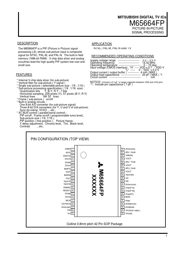
PIN CONFIGURATION (TOP VIEW)
SWM ACK SDATA SCLK DVdd DVss BGPS SCK BGPM FSC TEST5 TEST6 SWMG RESET DVdd DVss MCK CSYNCS AVss(ad) Vrb Vrt
1 2 3 4 5 6 7 8 9 10 11 12 13 14 15 16 17 18 19 20 21 42 41 40 39 38 37...