M68762SL
M68762SL is Silicon Bipolar Power Amplifier manufactured by Mitsubishi Electric.
MITSUBISHI RF POWER MODULE
Silicon Bipolar Power Amplifier, 350-400MHz 30W FM Mobile
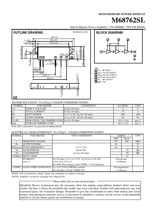
OUTLINE DRAWING
66+/-0.5 3+/-0.3 7.25+/-0.8 60+/-0.5 51.5+/-0.5
Dimensions in mm
BLOCK DIAGRAM
2 3 4
21+/-0.5
1.5+0.8/-0
21.5+/-0.5
22.5+/-0.5
4+/-0.3
5 6
2-R2+/-0.5 1
10+/-0.5
2 phi 0.45 +/-0.2
12+/-1 16.5+/-1
7.5+0.8/-0
14+/-1
33.0+/-1 43.5+/-1 55.5+/-1
PIN: 1 Pin : RF INPUT 2 Vcc1: 1st. DC SUPPLY 3 Vcc2: 2nd. DC SUPPLY 4 Vcc3: 3rd. DC SUPPLY 5 Po : RF OUTPUT 6 GND : FIN
(9.8)
H3
MAXIMUM RATINGS (Tc=25deg C UNLESS OTHERWISE NOTED)
SYMBOL PARAMETER Vcc SUPPLY VOLTAGE Icc TOTAL CURRENT Pin INPUT POWER Po OUTPUT POWER Tc(OP) OPERATION CASE TEMPERATURE Tstg STORAGE TEMPERATURE Note:Above parameters are guaranteed independently. CONDITIONS ZG=ZL=50 ohms ZG=ZL=50 ohms Vcc1<12.5V, ZG=ZL=50 ohms Vcc1<12.5V, ZG=ZL=50 ohms ZG=ZL=50 ohms RATINGS 17 10 600 40 -30 to +110 -40 to +110 UNIT V A m W W deg. C deg. C
ELECTRICAL CHARACTERISTICS (Tc=25deg.C UNLESS OTHERWISE NOTED)
SYMBOL f Po Efficiency 2fo 3fo VSWR in PARAMETER FREQUENCY RANGE OUTPUT POWER TOTAL EFFICIENCY 2nd HARMONIC 3rd HARMONIC INPUT VSWR STABILITY (note 1) TEST CONDITIONS LIMITS MIN MAX 350 400 30 40 -30 -30 3.5 No parasitic oscillation No degradation or destroy UNIT MHz W % d Bc d Bc
- 3.1+/-0.4
VCC=12.5V, Pin=0.3W, ZG=ZL=50 ohms
ZG=50 ohms, VCC1=5-12.5V, Vcc2=Vcc3=10-16V (Vcc1<Vcc2=Vcc3) Po<40W (Pin control), Load VSWR < 3.0:1(all phase) VSWRT LOAD VSWR TOLERANCE VCC=15.2V,Po=30W(Pin control) ZG=50 ohms, LOAD VSWR=20:1 NOTE: Above parameters, ratings, limits and conditions are subject to change. NOTE1: Stability is tested by sampling test (10pcs/LOT)
2.3+/-0.3
- Keep safety first in your circuit designs! Mitsubishi Electric Corporation puts the maximum effort into making semiconductor products better and more reliable, but there is always the possibility that trouble may occur with them. Trouble with semiconductors may lead to personal injury, fire or property damage. Remember...