V58C365164S
V58C365164S is 64 Mbit DDR SDRAM 4M X 16/ 3.3VOLT manufactured by Mosel Vitelic Corp.
MOSEL VITELIC
V58C365164S 64 Mbit DDR SDRAM 4M X 16, 3.3VOLT
PRELIMINARY
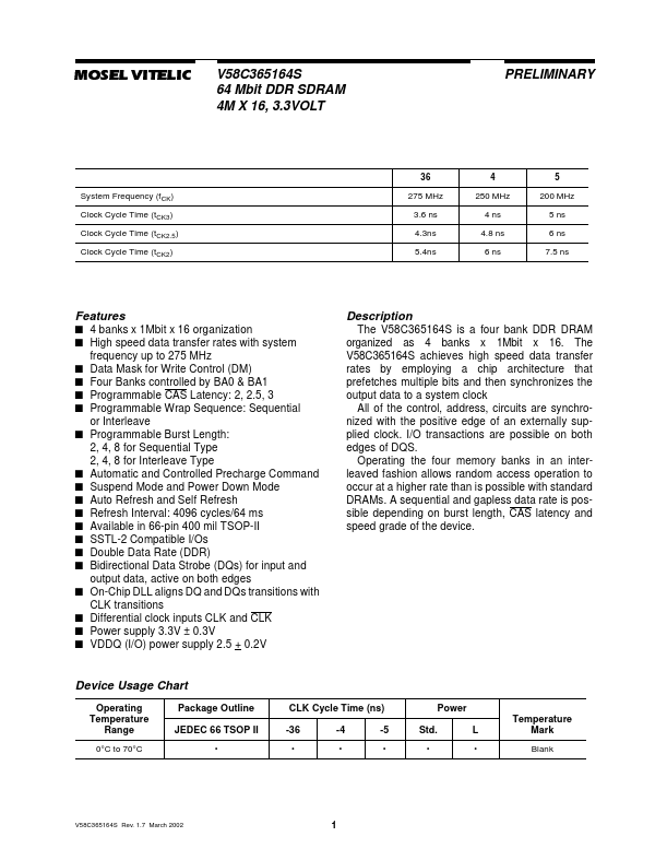
36 System Frequency (fCK) Clock Cycle Time (tCK3) Clock Cycle Time (tCK2.5) Clock Cycle Time (tCK2) 275 MHz 3.6 ns 4.3ns 5.4ns
4 250 MHz 4 ns 4.8 ns 6 ns
5 200 MHz 5 ns 6 ns 7.5 ns
Features
- 4 banks x 1Mbit x 16 organization
- High speed data transfer rates with system frequency up to 275 MHz
- Data Mask for Write Control (DM)
- Four Banks controlled by BA0 & BA1
- Programmable CAS Latency: 2, 2.5, 3
- Programmable Wrap Sequence: Sequential or Interleave
- Programmable Burst Length: 2, 4, 8 for Sequential Type 2, 4, 8 for Interleave Type
- Automatic and Controlled Precharge mand
- Suspend Mode and Power Down...