Datasheet Summary
MOTOROLA
SEMICONDUCTOR TECHNICAL DATA
Order this document by BCW29LT1/D
General Purpose Transistors
PNP Silicon
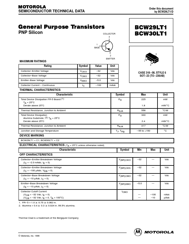
COLLECTOR 3 1 BASE 2 EMITTER
BCW29LT1 BCW30LT1
3 1
MAXIMUM RATINGS
Rating Collector- Emitter Voltage Collector- Base Voltage Emitter- Base Voltage Collector Current
- Continuous Symbol VCEO VCBO VEBO IC Value
- 32
- 32
- 5.0
- 100 Unit Vdc Vdc Vdc mAdc
CASE 318
- 08, STYLE 6 SOT- 23 (TO
- 236AB)
THERMAL CHARACTERISTICS
Characteristic Total Device Dissipation FR-5 Board (1) TA = 25°C Derate above 25°C Thermal Resistance, Junction to Ambient Total Device Dissipation Alumina Substrate, (2) TA = 25°C Derate above 25°C Thermal Resistance, Junction to Ambient Junction and Storage...