Datasheet Summary
BCW30LT1 General Purpose Transistors
PNP Silicon http://onsemi.
MAXIMUM RATINGS
Rating Collector-Emitter Voltage Collector-Base Voltage Emitter-Base Voltage Collector Current
- Continuous Symbol VCEO VCBO VEBO IC Value
- 32
- 32
- 5.0
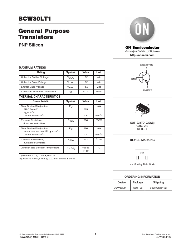
- 100 Unit Vdc Vdc Vdc mAdc 1 BASE
COLLECTOR 3
2 EMITTER
THERMAL CHARACTERISTICS
Characteristic Total Device Dissipation FR-5 Board(1) TA = 25°C Derate above 25°C Thermal Resistance, Junction to Ambient Total Device Dissipation Alumina Substrate,(2) TA = 25°C Derate above 25°C Thermal Resistance, Junction to Ambient Junction and Storage Temperature (1) FR- 5 = 1.0 0.75 (2) Alumina = 0.4 0.3 Symbol PD 225 1.8 RθJA PD 556 300 2.4 RθJA TJ, Tstg 417
- 55 to...