BCW60DLT1
BCW60DLT1 is General Purpose Transistors manufactured by Motorola Semiconductor.
MOTOROLA
SEMICONDUCTOR TECHNICAL DATA
Order this document by BCW60ALT1/D
General Purpose Transistors
NPN Silicon
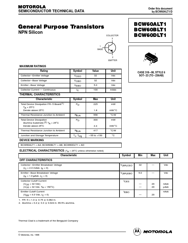
COLLECTOR 3 1 BASE
BCW60ALT1 BCW60BLT1 BCW60DLT1
2 EMITTER
1 2
MAXIMUM RATINGS
Rating Collector
- Emitter Voltage Collector
- Base Voltage Emitter
- Base Voltage Collector Current
- Continuous Symbol VCEO VCBO VEBO IC Value 32 32 5.0 100 Unit Vdc Vdc Vdc m Adc
CASE 318
- 08, STYLE 6 SOT- 23 (TO
- 236AB)
THERMAL CHARACTERISTICS
Characteristic Total Device Dissipation FR- 5 Board(1) TA = 25°C Derate above 25°C Thermal Resistance Junction to Ambient Total Device Dissipation Alumina Substrate,(2) TA = 25°C Derate above 25°C Thermal Resistance Junction to Ambient Junction and Storage Temperature Symbol PD Max 225 1.8 Rq JA PD 556 300 2.4 Rq JA TJ, Tstg 417
- 55 to +150 Unit m W m W/°C °C/W m W m W/°C °C/W °C
DEVICE MARKING
BCW60ALT1 = AA, BCW60BLT1 = AB, BCW60DLT1 = AD
ELECTRICAL CHARACTERISTICS (TA = 25°C unless otherwise noted)
Characteristic Symbol Min Max Unit
OFF CHARACTERISTICS
Collector
- Emitter Breakdown Voltage (IC = 2.0 m Adc, IE = 0) Emitter
- Base Breakdown Voltage (IE = 1.0 m Adc, IC = 0) Collector Cutoff Current (VCE = 32 Vdc) (VCE = 32 Vdc, TA = 150°C) Emitter Cutoff Current (VEB = 4.0 Vdc, IC = 0) 1. FR- 5 = 1.0 0.75 2. Alumina = 0.4 0.3 V(BR)CEO V(BR)EBO ICES
- - IEBO
- 20 20 20 n Adc µAdc n Adc 32 5.0
- - Vdc Vdc
0.062 in. 0.024 in. 99.5% alumina.
Thermal Clad is a trademark of the Bergquist pany
Motorola Small- Signal Transistors, FETs and Diodes Device Data © Motorola, Inc. 1996
BCW60ALT1 BCW60BLT1 BCW60DLT1
ELECTRICAL CHARACTERISTICS (TA = 25°C unless otherwise noted)...