BSV52LT1 Datasheet Text
MOTOROLA
SEMICONDUCTOR TECHNICAL DATA
Order this document by BSV52LT1/D
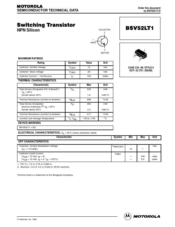
Switching Transistor
NPN Silicon
1 BASE
COLLECTOR 3
BSV52LT1
2 EMITTER
3 1 2
MAXIMUM RATINGS
Rating Collector
- Emitter Voltage Collector
- Base Voltage Collector Current
- Continuous Symbol VCEO VCBO IC Value 12 20 100 Unit Vdc Vdc mAdc
CASE 318
- 08, STYLE 6 SOT- 23 (TO
- 236AB)
THERMAL CHARACTERISTICS
Characteristic Total Device Dissipation FR- 5 Board(1) TA = 25°C Derate above 25°C Thermal Resistance Junction to Ambient Total Device Dissipation Alumina Substrate,(2) TA = 25°C Derate above 25°C Thermal Resistance Junction to Ambient Junction and Storage Temperature Symbol PD Max 225 1.8 RqJA PD 556 300 2.4 RqJA TJ, Tstg 417
- 55 to +150 Unit mW mW/°C °C/W mW mW/°C °C/W °C
DEVICE MARKING
BSV52LT1 = B2
ELECTRICAL CHARACTERISTICS (TA = 25°C unless otherwise noted)
Characteristic Symbol Min Max Unit
OFF CHARACTERISTICS
Collector
- Emitter Breakdown Voltage (IC = 1.0 mAdc) Collector Cutoff Current (VCB = 10 Vdc, IE = 0) (VCB = 10 Vdc, IE = 0, TA = 125°C) 1. FR- 5 = 1.0 0.75 2. Alumina = 0.4 0.3 V(BR)CEO 12 ICBO
- - 100 5.0 nAdc µAdc
- Vdc...