BSV52LT1 Datasheet Text
..
BSV52LT1 Switching Transistor
NPN Silicon
Features
- Pb- Free Package is Available
MAXIMUM RATINGS
Rating Collector
- Emitter Voltage Collector
- Base Voltage Collector Current
- Continuous Symbol VCEO VCBO IC Value 12 20 100 Unit Vdc Vdc mAdc http://onsemi.
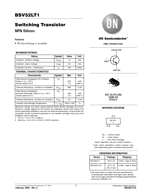
COLLECTOR 3 1 BASE 2 EMITTER
THERMAL CHARACTERISTICS
Characteristic Total Device Dissipation FR- 5 Board, (Note 1) TA = 25°C Derate above 25°C Thermal Resistance, Junction- to- Ambient Total Device Dissipation Alumina Substrate, (Note 2) TA = 25°C Derate above 25°C Thermal Resistance, Junction- to- Ambient Junction and Storage Temperature Symbol PD 225 1.8 RqJA PD 300 2.4 RqJA TJ, Tstg 417
- 55 to +150 mW mW/°C °C/W °C 556 mW mW/°C °C/W 1 2 Max Unit
3
SOT- 23 (TO- 236) CASE 318 STYLE 6
Maximum ratings are those values beyond which device damage can occur. Maximum ratings applied to the device are individual stress limit values (not normal operating conditions) and are not valid simultaneously. If these limits are exceeded, device functional operation is not implied, damage may occur and reliability may be affected. 1. FR- 5 = 1.0 x 0.75 x 0.062 in. 2. Alumina = 0.4 x 0.3 x 0.024 in. 99.5% alumina.
MARKING DIAGRAM
B2 M G G 1
B2 = Device Code M = Date Code- G = Pb- Free Package (Note: Microdot may be in either location)
- Date Code orientation and/or overbar may vary depending upon manufacturing location.
ORDERING INFORMATION
Device BSV52LT1 BSV52LT1G Package SOT- 23 SOT- 23 (Pb- Free) Shipping † 3,000 / Tape & Reel 3,000 / Tape & Reel
†For information on tape and reel specifications, including part orientation and tape sizes, please refer to our Tape and Reel Packaging Specifications Brochure, BRD8011/D.
© Semiconductor ponents Industries, LLC, 2006
1
February, 2006
- Rev. 2
Publication...