J112
Overview
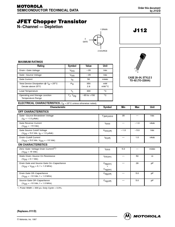
MOTOROLA SEMICONDUCTOR TECHNICAL DATA Order this document by J112/D JFET Chopper Transistor N–Channel — Depletion 1 DRAIN 3 GATE J112 2 SOURCE MAXIMUM RATINGS Rating Drain – Gate Voltage Gate – ...
| Part | J112 |
|---|---|
| Description | JFET Chopper Transistor |
| Category | Transistor |
| Manufacturer | Motorola Semiconductor |
| Size | 110.90 KB |
MOTOROLA SEMICONDUCTOR TECHNICAL DATA Order this document by J112/D JFET Chopper Transistor N–Channel — Depletion 1 DRAIN 3 GATE J112 2 SOURCE MAXIMUM RATINGS Rating Drain – Gate Voltage Gate – ...