Datasheet4U Logo Datasheet4U.com

MPC958 - LOW VOLTAGE PLL CLOCK DRIVER

Key Features

  • make the MPC958 ideal for use as a zero delay, low skew fanout buffer. The device performance has been tuned and optimized for zero delay performance. The MR/OE input pin will tristate the output buffers when driven “high”. The MPC958 is fully 3.3V compatible and requires no external loop filter components. All control inputs accept LVCMOS or LVTTL compatible levels while the outputs provide LVCMOS levels with the ability to drive terminated 50Ω transmission lines. For series terminated 50Ω line.

📥 Download Datasheet

Full PDF Text Transcription (Reference)

The following content is an automatically extracted verbatim text from the original manufacturer datasheet and is provided for reference purposes only.

View original datasheet text
MOTOROLA Freescale Semiconductor, Inc. SEMICONDUCTOR TECHNICAL DATA Order this document by MPC958/D Low Voltage PLL Clock Driver
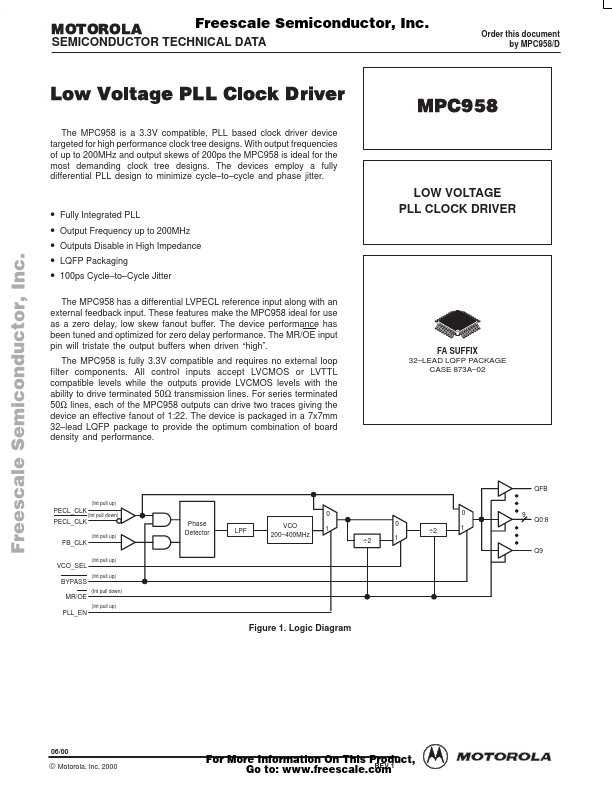
 The MPC958 is a 3.3V compatible, PLL based clock driver device targeted for high performance clock tree designs. With output frequencies of up to 200MHz and output skews of 200ps the MPC958 is ideal for the most demanding clock tree designs. The devices employ a fully differential PLL design to minimize cycle–to–cycle and phase jitter. MPC958 • Fully Integrated PLL • Output Frequency up to 200MHz LOW VOLTAGE PLL CLOCK DRIVER Freescale Semiconductor, Inc... • Outputs Disable in High Impedance • LQFP Packaging • 100ps Cycle–to–Cycle Jitter The MPC958 has a differential LVPECL reference input along with an external feedback input.