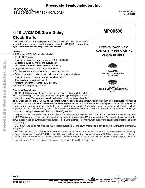
MPC9608 Overview
Key Specifications
Package: TQFP
Mount Type: Surface Mount
Pins: 32
Operating Voltage: 3.3 V
Key Features
- 1:10 outputs LVCMOS zero-delay buffer Freescale Semiconductor, Inc
| Part | MPC9608 |
|---|---|
| Description | 1:10 LVCMOS Zero Delay Clock Buffer |
| Manufacturer | Motorola Semiconductor |
| Size | 463.08 KB |
Package: TQFP
Mount Type: Surface Mount
Pins: 32
Operating Voltage: 3.3 V
| Seller | Inventory | Price Breaks | Buy |
|---|---|---|---|
| Antdic Electronics | 24050 | 1+ : 4 USD 10+ : 3.8 USD 100+ : 3.6 USD 1000+ : 3.2 USD |
View Offer |
| ICPartonline | 13582 | 1+ : 25 USD 10+ : 23.75 USD 100+ : 22.5 USD 1000+ : 21.25 USD |
View Offer |
| Part Number | Manufacturer | Description |
|---|---|---|
| MPC9600 | Motorola Semiconductor | LOW VOLTAGE 2.5 V AND 3.3 V CMOS PLL CLOCK DRIVER |