2N2720
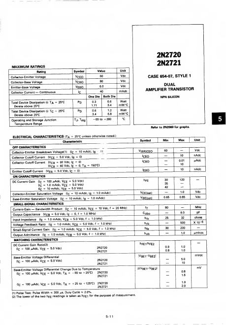
2N2720 is DUAL AMPLIFIER TRANSISTOR manufactured by Motorola Semiconductor.
MAXIMUM RATINGS
Rating Collector-Emitter Voltage Collector-Base Voltage Emitter-Base Voltage
- Collector Current Continuous
@ Total Device Dissipation TA = 25°C
Derate above 25°C
@ Total Device Dissipation Tc = 25°C
Derate above 25°C Operating and Storage Junction
Temperature Range
Symbol VCEO VCBO VEBO ic
PD pd
Tj. Tstg
Value
One Die Both Die
- 65 to + 200
Unit Vdc Vdc Vdc m Adc
Watt m W/°C Watt m W/°C
°C
2N2720 2N2721
CASE 654-07, STYLE 1 DUAL
AMPLIFIER TRANSISTOR
NPN SILICON
Refer to 2N2060 for graphs.
ELECTRICAL CHARACTERISTICS (TA = 25°C unless otherwise noted.)
Characteristic
OFF CHARACTERISTICS
Collector-Emitter Breakdown Voltaged) 0c = 10 m Adc, Bl 0)_
Collector Cutoff Current Collector Cutoff Current
(VCE = 5.0 Vdc, I.b =...


