Motorola 2N5656
POWER TRANSISTORS
| Part No. | 2N5656 |
|---|---|
| Datasheet | 2N5656 Download |
| Manufacturer |  Motorola |
| Description | POWER TRANSISTORS |
| Buy | Stock & Price |
MAXIMUM RATINGS
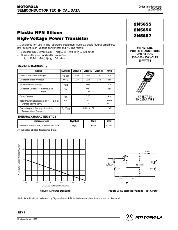
(1) Rating Symbol VCEO VCB VEB IC IB 2N5655 250 275 2N5656 300 325 6.0 0.5 1.0 2N5657 350 375 Unit Vdc Vdc Vdc Adc Adc Collector–Emitter Voltage Collector–Base Voltage Emitter–Base Voltage Collector Current — Continuous Peak Base Current 0.25 Total Power Dissipation @ TC = 25_ C Derate above 25_ C Operating and Storage Junction Temperature Range PD 20 0.16 Watts W/_ C _C . . . designed for use in line–operated equipment such as audio output amplifiers; low–current, high–voltage converters; and AC line relays. CASE 77–08 TO–225AA TYPE TJ, Tstg – 65 to + 150 THERMAL CHARACTERISTICS Characteristic Symbol θJC Max Unit Thermal Resistance, Junction to Case 6.25 _ C/W (1) Indicates JEDEC Registered Data. 40 PD, POWER DISSIPATION (WATTS) 30 50 mH 20 Hg RELAY X 200 TO SCOPE + 6.0 V Y + 50 V – 10 300 1.0 0 25 50 75 100 TC, CASE TEMPERATURE (°C) 125 150 Figure 1. Power Derating Figure 2. Sustaining Voltage Test Circuit Safe Area Limits are indicated by Figures 3 and 4. Both limits are applicable and must be observed.