74LS399
features both Q and Q inputs, while the SN54 / 74LS399 has only Q outputs.
- Select From Two Data Sources
- Fully Positive Edge-Triggered Operation
- Both True and plemented Outputs on SN54 / 74LS398
- Input Clamp Diodes Limit High-Speed Termination Effects
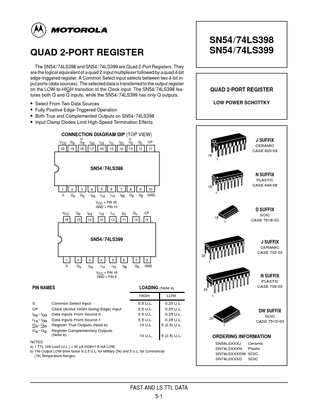
CONNECTION DIAGRAM DIP (TOP VIEW) VCC Qd Qd Iod I1d I1c I0c Qc Qc CP 20 19 18 17 16 15 14 13 12 11
SN54 / 74LS398
1 2 3 4 5 6 7 8 9 10 S Qa Qa I0a I1a I1b I0b Qb Qb GND
VCC = PIN 20 GND = PIN 10 VCC Qd I0d I1d I1c I0c Qc CP 16 15 14 13 12 11 10 9
SN54 / 74LS399
1 2 3 4 56 78 S Qa I0a I1a I1b I0b Qb GND
VCC = PIN 16 GND = PIN 8
PIN NAMES
LOADING (Note a)
HIGH
I0a
- I0d I1a
- I0d Qa
- Qd Qa
- Qd mon Select Input Clock (Active HIGH Going Edge) Input Data Inputs From Source 0 Data Inputs From Source 1 Register True Outputs (Note b) Register plementary Outputs (Note b)
0.5 U.L. 0.5 U.L. 0.5 U.L. 0.5 U.L. 10 U.L.
10 U.L.
0.25 U.L. 0.25 U.L. 0.25 U.L. 0.25 U.L. 5 (2.5) U.L.
5 (2.5) U.L.
NOTES: a) 1 TTL Unit Load (U.L.)...