Motorola BFS17
RF TRANSISTOR
| Part No. | BFS17 |
|---|---|
| Datasheet | BFS17 Download |
| Manufacturer |  Motorola |
| Description | RF TRANSISTOR |
| Buy | Stock & Price |
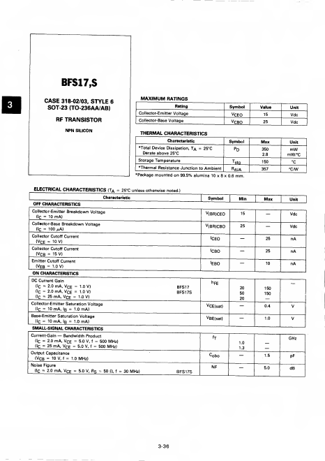
MAXIMUM RATINGS
Rating Collector-Emitter Voltage Collector-Base Voltage Symbol vCEO vCBO THERMAL CHARACTERISTICS Characteristic●Total Device Dissipation, T/\ = 25°C Derate above 25°C Symbol PD Storage Temperature Tstg Thermal Resistance Junction to Ambient R 0JA mm●Package mounted on 99.5% alumina 10 x 8 x 0.6