Motorola BS170
N-channel MOSFET
| Part No. | BS170 |
|---|---|
| Datasheet | BS170 Download |
| Manufacturer |  Motorola |
| Description | N-channel MOSFET |
| Buy | Stock & Price |
MAXIMUM RATINGS
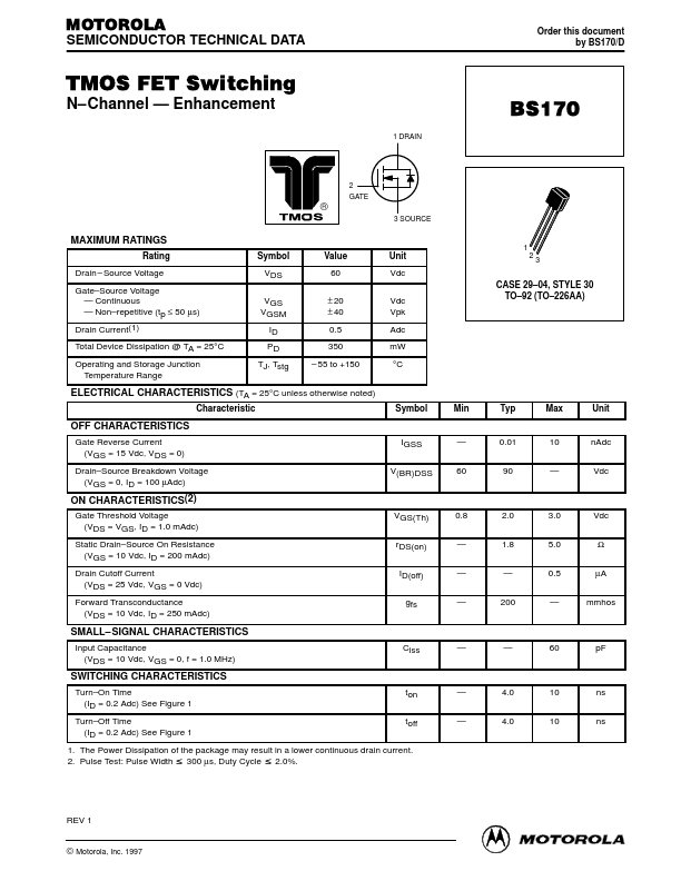
Rating Drain – Source Voltage Gate–Source Voltage — Continuous — Non–repetitive (tp ≤ 50 µs) Drain Current(1) Total Device Dissipation @ TA = 25°C Operating and Storage Junction Temperature Range Symbol VDS VGS VGSM ID PD TJ, Tstg Value 60 ± 20 ± 40 0.5 350 1 Unit Vdc Vdc Vpk Adc mW °C 2 3 CASE 29–04, STYLE 30 TO–92 (TO–226AA) – 55 to +150ELECTRICAL CHARACTERISTICS
(TA = 25°C unless otherwise noted) Characteristic Symbol Min Typ Max Unit OFF CHARACTERISTICS Gate Reverse Current (VGS = 15 Vdc, VDS = 0) Drain–Source Breakdown Voltage (VGS = 0, ID = 100 µAdc) IGSS V(BR)DSS — 60 0.01 90 10 — nAdc Vdc ON CHARACTERISTICS(2) Gate Threshold Voltage (VDS = VGS, ID = 1.0 mAdc) Static Drain–Source On Resistance (VGS = 10 Vdc, ID = 200 mAdc) Drain Cutoff Current (VDS = 25 Vdc, VGS = 0 Vdc) Forward Transconductance (VDS = 10 Vdc, ID = 250 mAdc) VGS(Th) rDS(on) ID(off) gfs 0.8 — — — 2.0 1.8 — 200 3.0 5.0 0.5 — Vdc Ω µA mmhos SMALL– SIGNAL CHARACTERISTICS Input Capacitance (VDS = 10...