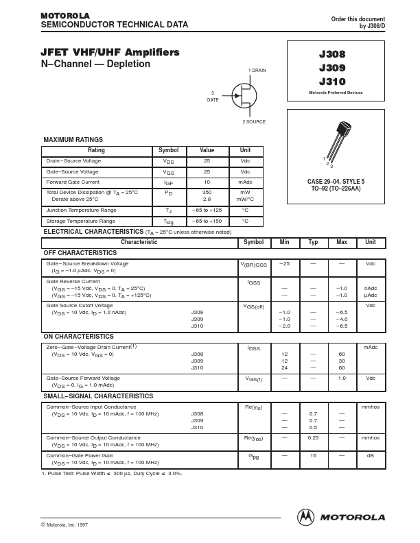
J310 Overview
Key Specifications
Representative J310 image (package may vary by manufacturer)
Key Features
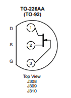
- Source Voltage Gate
- Source Voltage Forward Gate Current Total Device Dissipation @ TA = 25°C Derate above 25°C Junction Temperature Range Storage Temperature Range Symbol VDS VGS IGF PD TJ Tstg Value 25 25 10 350 2.8