Motorola MC10E150
The MC10E/100E150 contains six D-type latches with differential outputs. When both Latch Enables (LEN1, LEN2) are LOW, the latch is transparent and input data transitions propagate through to the output. The Master Reset (MR) overrides all other controls to set the Q outputs low.| Part No. | MC10E150 |
|---|---|
| Datasheet | MC10E150 Download |
| Manufacturer |  Motorola |
| Description | 6-BIT D LATCH |
| Buy | Stock & Price |

MOTOROLA SEMICONDUCTOR TECHNICAL DATA 6ĆBit D Latch A logic HIGH on either LEN1 or LEN2 (or both) latches the data.
● 800ps Max. Propagation Delay
● Extended 100E VEE Range of – 4.2V to – 5.46V
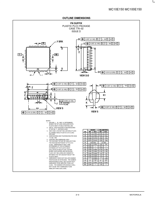
● 75kΩ Input Pulldown Resistors LOGIC DIAGRAM D0 D Q0 R Q0 MC10E150 MC100E150 6-BIT D LATCH D1 D Q1 R Q1 D2 D Q2 R Q2 FN SUFFIX PLASTIC PACKAGE CASE 776-02 D3 D Q3 R Q3 D4 D Q4 R Q4 D5 D Q5 R Q5 LEN1 LEN2 MR PIN NAMES Pin D0 – D5 LEN1, LEN2 MR Q0 – Q5 Q0 – Q5 Function Data Inputs Latch Enables Master Reset True Outputs Inverting Outputs 12/93 © Motorola, Inc. 1996 2–1 Pinout: 28-Lead PLCC (Top View) MR LEN2 LEN1 NC VCCO Q5 Q5 25 24 23 22 21 20 19 D5 26 18 Q4 D4 27