MC14511B
Overview
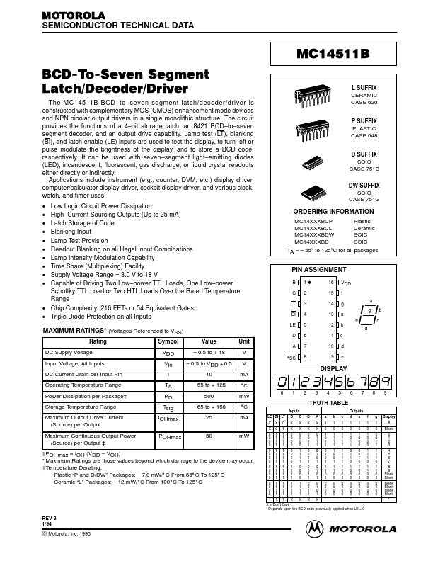
MOTOROLA SEMICONDUCTOR TECHNICAL DATA MC14511B BCD-To-Seven Segment Latch/Decoder/Driver The MC14511B BCD–to–seven segment latch/decoder/driver is constructed with complementary MOS (CMOS) enhanceme...
| Part | MC14511B |
|---|---|
| Description | BCD-To-Seven Segment Latch/Decoder/Driver |
| Manufacturer | Motorola Semiconductor |
| Size | 248.98 KB |
MOTOROLA SEMICONDUCTOR TECHNICAL DATA MC14511B BCD-To-Seven Segment Latch/Decoder/Driver The MC14511B BCD–to–seven segment latch/decoder/driver is constructed with complementary MOS (CMOS) enhanceme...
| Part Number | Manufacturer | Description |
|---|---|---|
| MC14511B | onsemi | BCD-To-Seven Segment Latch/Decoder/Driver |
| MC14511 | Unisonic Technologies | BCD-TO-SEVEN SEGMENT LATCH/DECODER/DRIVER |
| MC14515 | onsemi | 4-Bit Transparent Latch/4-to-16 Line Decoder |
| MC14513B | onsemi | BCD-To-Seven Segment Latch/Decoder/Driver |
| MC14517B | onsemi | Dual 64-Bit Static Shift Register |