Datasheet4U Logo Datasheet4U.com

MCM36F9 - 1MB and 2MB Synchronous Fast Static RAM Module

Description

Pin Locations 3, 4, 5, 6, 7, 8, 17, 18, 19, 20, 21, 22, 27, 28, 29, 30, 31, 32 82 39, 40, 103, 104 73, 74, 141, 142 (a) 49, 50, 53, 54, 55, 56, 57, 58, (b) 63, 64, 65, 66, 69, 70, 71, 72 (c) 109, 110, 111, 112, 125, 126, 129, 130 (d) 131, 132, 133, 134, 135, 136, 139, 140 41, 105 42, 106 46, 45, 12

Features

  • = 0 to 70°C, Unless Otherwise Noted) Input Timing Measurement Reference Level.
  • . . . . 1.25 V Input Pulse Levels.
  • . . . 0 to 2.5 V Input Rise/Fall Time.
  • . . . 1 V/ns (20 to 80%) Output Timing Reference Level.
  • 1.25 V Output Load.
  • . . . . See Figure 1 Unless Otherwise Noted DATA RAM READ/WRITE CYCLE TIMING (See Notes 1, 2, 3, and 4).

📥 Download Datasheet

Datasheet preview – MCM36F9

Datasheet Details

Part number MCM36F9
Manufacturer Motorola
File Size 123.43 KB
Description 1MB and 2MB Synchronous Fast Static RAM Module
Datasheet download datasheet MCM36F9 Datasheet
Additional preview pages of the MCM36F9 datasheet.
Other Datasheets by Motorola

Full PDF Text Transcription

Click to expand full text
MOTOROLA SEMICONDUCTOR TECHNICAL DATA Order this document by MCM36F8/D Advance Information 1MB and 2MB Synchronous Fast Static RAM Module 
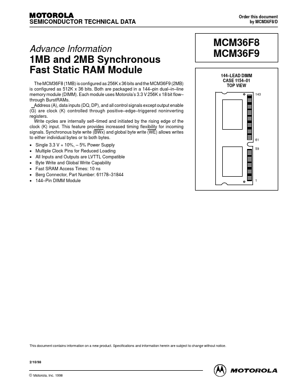
The MCM36F8 (1MB) is configured as 256K x 36 bits and the MCM36F9 (2MB) is configured as 512K x 36 bits. Both are packaged in a 144–pin dual–in–line memory module (DIMM). Each module uses Motorola’s 3.3 V 256K x 18 bit flow– through BurstRAMs. Address (A), data inputs (DQ, DP), and all control signals except output enable (G) are clock (K) controlled through positive–edge–triggered noninverting registers. Write cycles are internally self–timed and initiated by the rising edge of the clock (K) input. This feature provides increased timing flexibility for incoming signals.
Published: |