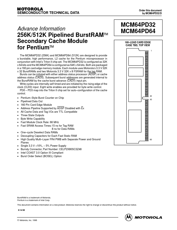
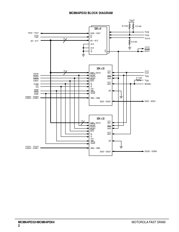
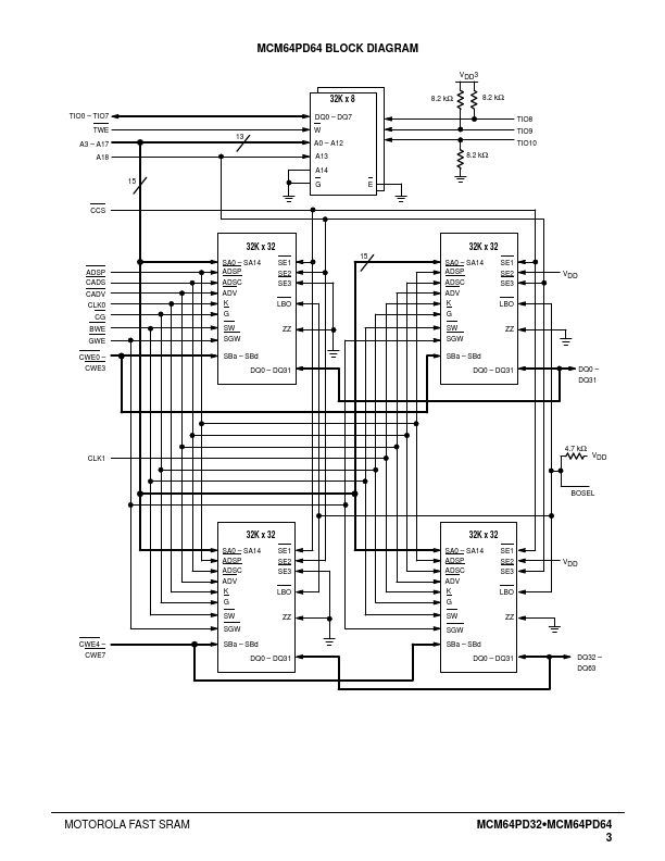
Datasheet4U Logo Datasheet4U.com

MCM64PD32 - 256K/512K Pipelined BurstRAM Secondary Cache Module for Pentium

General Description

160 Lead Card Edge Pin Locations 20, 21, 22, 23, 24, 26, 28, 29, 101, 102, 103, 104, 106, 108, 109, 110 30 Symbol A3

A18 ADSP Type Input Input Description Address Inputs: These inputs are registered into data RAMs and must meet setup and hold times.

Key Features

  • meet the dc and ac specifications shown in the tables, after thermal equilibrium has been established. This device contains circuitry that will ensure the output devices are in High.
  • Z at power up. Tstg.
  • 65 to + 150 °C NOTE: Permanent device damage may occur if.

📥 Download Datasheet

Full PDF Text Transcription (Reference)

The following content is an automatically extracted verbatim text from the original manufacturer datasheet and is provided for reference purposes only.

View original datasheet text
MOTOROLA SEMICONDUCTOR TECHNICAL DATA Order this document by MCM64PD32/D Advance Information 256K/512K Pipelined BurstRAM™ Secondary Cache Module for Pentium™ The MCM64PD32 (256K) and MCM64PD64 (512K) are designed to provide a burstable, high performance, L2 cache for the Pentium microprocessor in conjunction with Intel’s Triton II chip set. The MCM64PD32 is configured as 32K x 64 bits and the MCM64PD64 is configured as 64K x 64 bits. Both are packaged in a 160 pin card edge memory module. Each module uses Motorola’s 3.3 V 32K x 32 BurstRAMs and two Motorola 3.3 V 32K x 8 FSRAM for the tag RAM. Bursts can be initiated with either address status processor (ADSP) or cache address status (CADS).