Datasheet4U Logo Datasheet4U.com

MMBF4391LT1 - JFET Switching Transistors

Key Features

  • completed, the device should be allowed to cool naturally for at least three minutes. Gradual cooling should be used as the use of forced cooling will increase the temperature gradient and result in latent failure due to mechanical stress.
  • Mechanical stress or shock should not be applied during cooling.
  • Soldering a device without preheating can cause excessive thermal shock and stress which can result in damage to the device. The values for the equation are found in the maximum.

📥 Download Datasheet

Full PDF Text Transcription (Reference)

The following content is an automatically extracted verbatim text from the original manufacturer datasheet and is provided for reference purposes only.

View original datasheet text
MOTOROLA SEMICONDUCTOR TECHNICAL DATA Order this document by MMBF4391LT1/D JFET Switching Transistors N–Channel 2 SOURCE 3 GATE MMBF4391LT1 MMBF4392LT1 MMBF4393LT1 3 1 1 DRAIN MAXIMUM RATINGS Rating Drain–
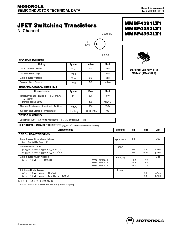
Source Voltage Drain–Gate Voltage Gate–Source Voltage Forward Gate Current Symbol VDS VDG VGS IG(f) Value 30 30 30 50 Unit Vdc Vdc Vdc mAdc 2 CASE 318 – 08, STYLE 10 SOT– 23 (TO – 236AB) THERMAL CHARACTERISTICS Characteristic Total Device Dissipation FR– 5 Board(1) TA = 25°C Derate above 25°C Thermal Resistance, Junction to Ambient Junction and Storage Temperature Symbol PD Max 225 1.