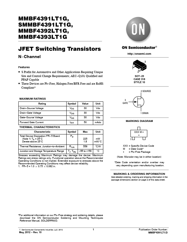
MMBF4391LT1G Overview
Key Features
- S Prefix for Automotive and Other Applications Requiring Unique Site and Control Change Requirements; AEC-Q101 Qualified and PPAP Capable
- These Devices are Pb-Free, Halogen Free/BFR Free and are RoHS Compliant*
| Part | MMBF4391LT1G |
|---|---|
| Description | JFET Switching Transistors |
| Category | Transistor |
| Manufacturer | onsemi |
| Size | 129.23 KB |
| Part Number | Manufacturer | Description |
|---|---|---|
| MMBF4391LT1 | Motorola Semiconductor | JFET Switching Transistors |
| MMBF4391 | Fairchild Semiconductor | N-Channel Switch |