MMBFJ175LT1
Overview
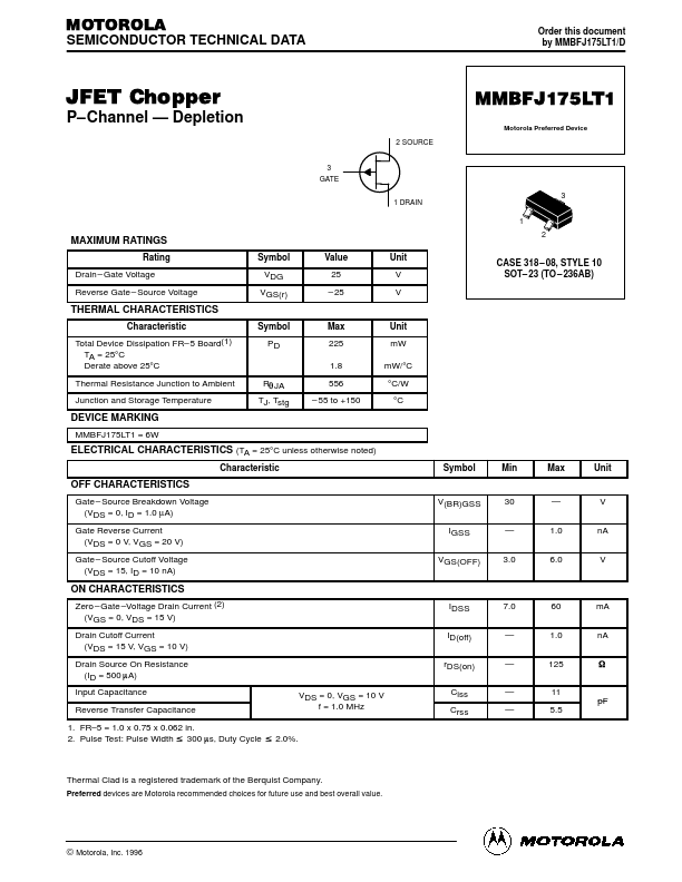
MOTOROLA SEMICONDUCTOR TECHNICAL DATA Order this document by MMBFJ175LT1/D JFET Chopper P–Channel — Depletion 2 SOURCE 3 GATE 1 DRAIN MMBFJ175LT1 Motorola Preferred Device 3 1 MAXIMUM RATINGS R...
| Part | MMBFJ175LT1 |
|---|---|
| Description | JFET Chopper |
| Manufacturer | Motorola Semiconductor |
| Size | 76.43 KB |
MOTOROLA SEMICONDUCTOR TECHNICAL DATA Order this document by MMBFJ175LT1/D JFET Chopper P–Channel — Depletion 2 SOURCE 3 GATE 1 DRAIN MMBFJ175LT1 Motorola Preferred Device 3 1 MAXIMUM RATINGS R...
| Part Number | Manufacturer | Description |
|---|---|---|
| MMBFJ175LT1G | onsemi | JFET Chopper |
| MMBFJ175LT1 | onsemi | JFET Chopper |
| MMBFJ175 | onsemi | P-Channel Switch |
| MMBFJ175 | Fairchild Semiconductor | P-Channel Switch |