MMBFJ175LT1
Overview
- Pb-Free Package is Available
| Part | MMBFJ175LT1 |
|---|---|
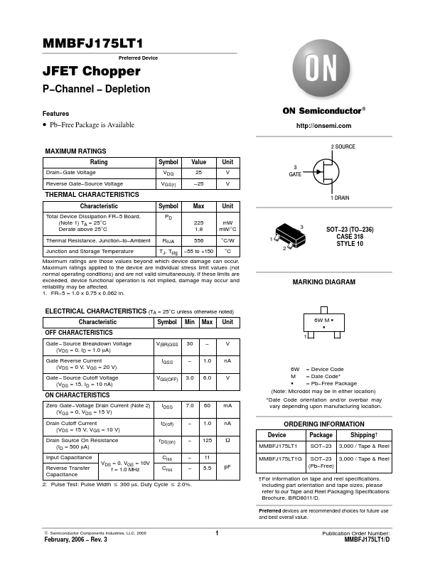
| Description | JFET Chopper |
| Manufacturer | onsemi |
| Size | 68.43 KB |
| Part Number | Manufacturer | Description |
|---|---|---|
| MMBFJ175LT1 | Motorola Semiconductor | JFET Chopper |
| MMBFJ175 | onsemi | P-Channel Switch |
| MMBFJ175 | Fairchild Semiconductor | P-Channel Switch |